A 4-layer laminated busbar designed for 800 V DC traction passed hi-pot and burned in clean, but PDIV on a random sample collapsed from 2.4 kV to 1.4 kV after the customer switched to SiC modules. A micro-focus CT scan found a 0.3 mm air pocket between PET film and inner copper, 2 mm from the conductor edge. Internal voids and delaminations do not show on a routine hipot — they quietly lower PDIV and feed treeing until the film punctures in the field. This guide walks through the three inspection routes, the tiered acceptance criteria, and the evidence package your supplier should already be handing you.
A 4-layer laminated busbar designed for 800 V DC traction passed hi-pot and burned in clean, but PDIV on a random sample collapsed from 2.4 kV to 1.4 kV after the customer switched to SiC modules. A micro-focus CT scan found a 0.3 mm air pocket between PET film and inner copper, 2 mm from the conductor edge. Internal voids and delaminations do not show on a routine hipot — they quietly lower PDIV and feed treeing until the film punctures in the field. This guide walks through the three inspection routes, the tiered acceptance criteria, and the evidence package your supplier should already be handing you.
A 4-layer laminated busbar 320 mm wide, designed for an 800 V DC traction drive, passed hi-pot at 3.5 kVAC and looked perfect on the bench. The first 200 units survived a 100 h burn-in. Then the customer swapped SiC modules in, switched the dead-time down to 80 ns, and the partial-discharge inception voltage (PDIV) measured on a random sample dropped from 2.4 kV to 1.4 kV. A micro-focus CT scan cut the mystery short: a 0.3 mm air pocket sat between the PET film and the inner copper foil, 2 mm from the conductor edge, exactly where the field crowding is worst.
Internal voids and delaminations inside a laminated busbar do not usually show up on a routine hipot. They fail quietly, by lowering the voltage at which partial discharge (PD) starts, and then by feeding electrical tree growth for months until the film punctures. This guide walks through where those voids come from, how to find them with X-ray CT, ultrasonic C-scan and PD testing, and what acceptance numbers to write into your drawing so your supplier cannot hand-wave the inspection away. If you have never audited a laminated busbar shop before, pair this read with our busbar quality-control inspection checklist before the first site visit.
A void is any trapped gas pocket larger than about 50 µm between two dielectric films or between film and copper. A delamination is a planar disbond that has spread laterally along an interface. Both are process problems, not material problems. Five root causes account for nearly every rejection we see in shop-floor feedback and in customer returns we have reverse-engineered.
Reading the manufacturing flow back from a CT or C-scan result is the fastest way to troubleshoot a lot. The laminated busbar manufacturing process walk-through shows where each of these steps sits on the press cycle.
A void by itself does not punch through a 0.25 mm PET film at 1,000 V DC. Air breaks down at roughly 30 kV/mm, PET at more like 150 kV/mm, so the gas pocket inside the laminate sees a much higher local field than the surrounding solid. The sequence that kills the part is the part you have to design around.
Step one: field enhancement. The dielectric constant of the film (εr ≈ 3.2 for PET, ≈ 2.1 for Nomex) is higher than air (εr ≈ 1.0). In series-capacitor terms, the electric field across the air pocket is amplified by the ratio of the permittivities — by roughly a factor of three right at the void. When that void sits at the conductor edge, where the geometric field is already 2–3× the uniform value, the local stress crosses 30 kV/mm long before the busbar's nominal working stress does.
Step two: partial discharge inception. Micro-discharges start inside the void, ionising the air and producing ozone and nitric acid that attack the PET surface. Step three: treeing. The erosion channels grow 5–50 µm per thousand hours of PD activity, dendritically, until a branch bridges two conductor layers. Step four: puncture. The time from first measurable pC to final breakdown in a busbar-grade PET laminate under constant PD stress is typically a few thousand hours — long enough to survive type test, short enough to fail in the field inside a warranty window.
That is why the acceptance number that actually matters is not the void size, but the PDIV margin above the working peak voltage. Our companion piece on partial-discharge-free busbar design works the design side; this article works the inspection side.
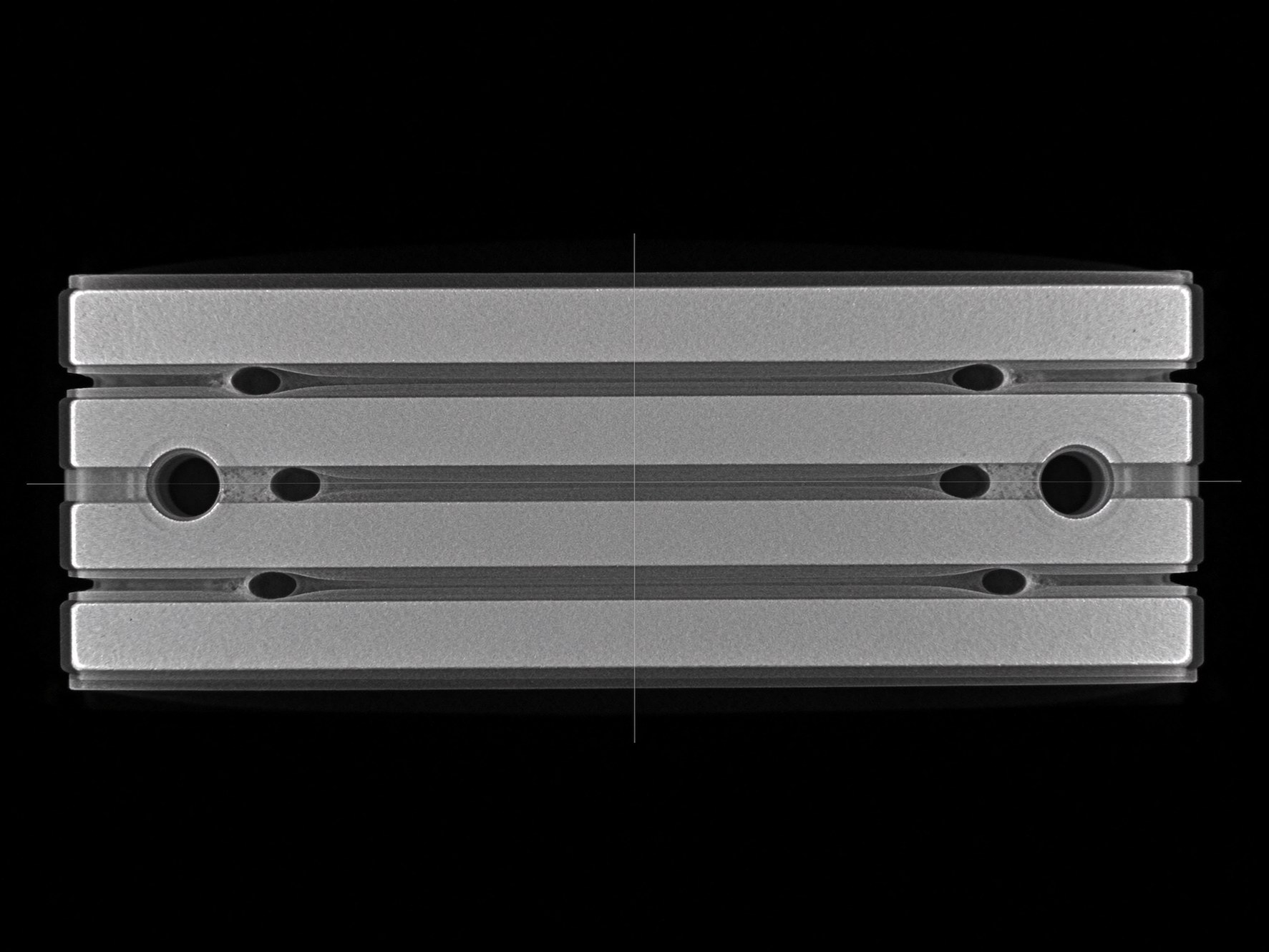
Industrial X-ray inspection comes in two flavours. Conventional 2D radiography projects the whole part onto a flat detector in one shot. You see every layer superimposed. A void between layer 2 and layer 3 overlaps with a punched hole in layer 4, and you cannot tell which is which. 2D X-ray catches gross misalignment, missing films and big copper-to-copper shorts, but it is the wrong tool for a 0.3 mm void hidden in a 6 mm stack.
Computed tomography (CT) rotates the part 360° on a stage, collects hundreds of projections, and reconstructs a voxel volume on which you can slice in any plane. Voxel size sets the resolution floor: for a busbar of 200–500 mm on a side, a micro-focus tube at 100–225 kVp typically delivers 50–100 µm isotropic voxels. You reliably resolve voids down to roughly 2–3× voxel size, i.e. about 0.15–0.25 mm. Anything smaller is hidden in the noise. ASTM E1695 (Standard Test Method for Measurement of Computed Tomography System Performance, current 2020 revision) spells out how to measure that resolution on a standardised tungsten wire phantom — ask your shop to include the wire-CT data sheet in the NDT package rather than just quoting a voxel number.
Reading CT slices is a skill. A well-trained NDT engineer scrolls through the stack layer by layer and flags voids by (a) equivalent circular diameter, (b) minimum distance to the nearest conductor edge, (c) whether the void touches any cut-out or outer edge, and (d) whether it is planar (delamination) or volumetric (bubble). Automated porosity software can list every pocket above a threshold, but a human still has to separate real voids from reconstruction artefacts at dense copper features.
CT does not come cheap. A single medium busbar on a 225 kVp micro-CT takes 15–45 minutes of scan time plus 5–15 minutes of reconstruction and report, and outsourced scan fees run on the order of several hundred US dollars per part. That economics drives the sampling strategy we come back to in Section 11.
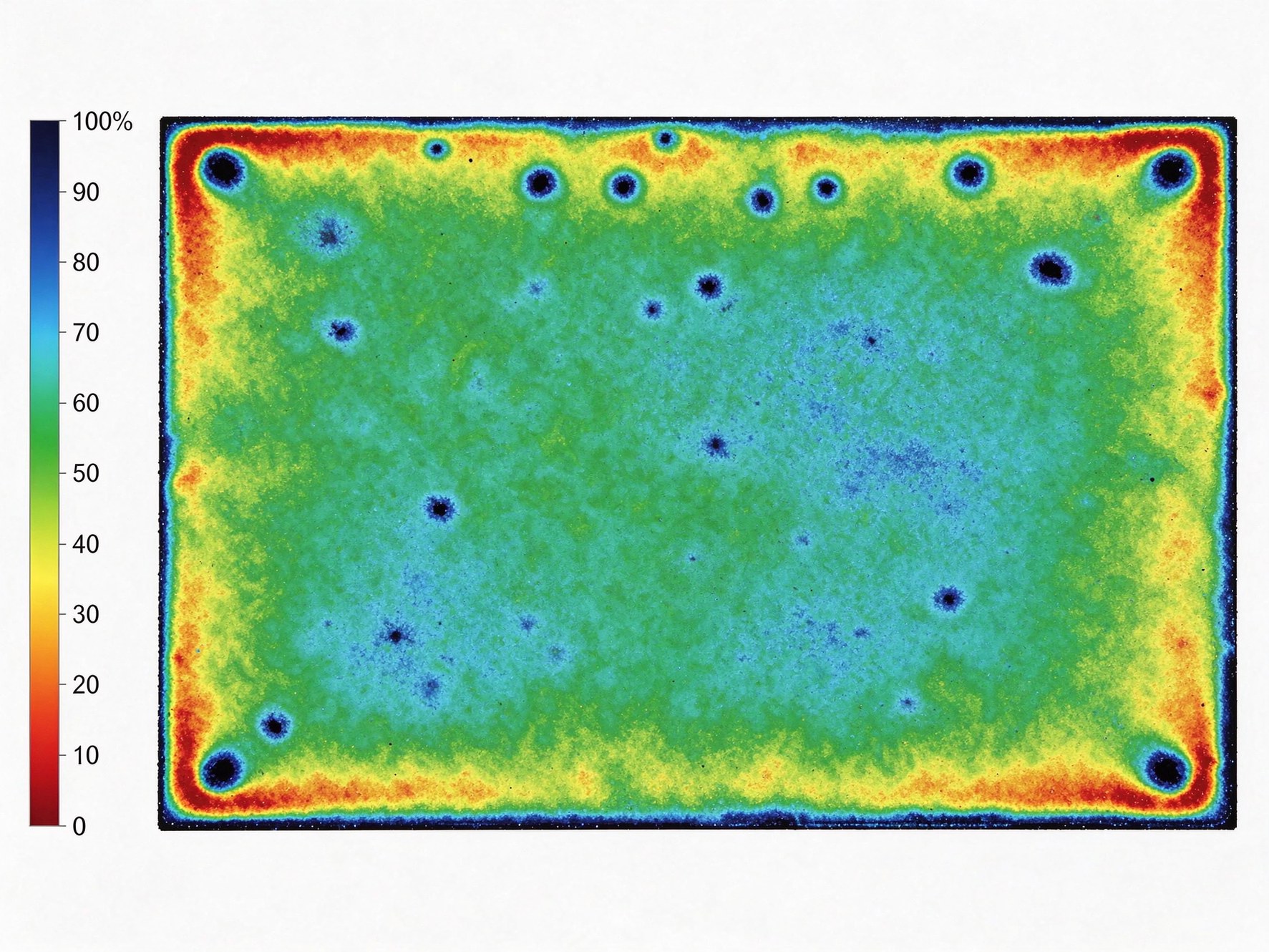
Ultrasonic testing (UT) is the workhorse for composite laminates, and it transfers well to laminated busbars. A 5–10 MHz focused transducer pulses water-coupled ultrasound into the top copper face. The sound wave travels through the copper, reflects off every acoustic impedance boundary, and returns. A well-bonded dielectric-to-copper interface gives a small, consistent back-wall echo. A delaminated or voided interface introduces an air gap (acoustic mismatch near 100 percent) and returns a much stronger front-face echo, with almost no signal reaching the back wall.
A C-scan rasterises the transducer across the part and plots the gated echo amplitude on a top-down colour map. The operator sets two gates: one around the front-surface echo, one around the expected copper-to-film interface echo. Delaminations show up as sudden, geometrically bounded colour blobs. Porosity clusters show up as speckle. Edge kiss-off (where the fillet resin did not wet) shows up as a continuous dark band along the perimeter.
UT's strengths: it is fast (a 400 × 300 mm busbar scans in 3–8 minutes), it is cheap, and it catches planar delaminations that CT can miss because the void gap is smaller than a voxel. Its weakness: copper attenuates high-frequency ultrasound, so on a 3 mm copper layer the resolution at the inner film drops; and UT cannot tell you the through-thickness position of a reflector without a B-scan. We use UT as the 100 percent screen, and CT as the follow-up on flagged units. The partial-discharge resource page and the UT reference in Section 13 are a good starting pair for writing an internal NDT spec.
Partial discharge testing is the only route that measures the electrical consequence of a void rather than the void itself. IEC 60270 (High-voltage test techniques — Partial discharge measurements, 2015 edition) defines the measurement loop: the test transformer supplies power-frequency (typically 50 or 60 Hz) or resonant AC voltage; a coupling capacitor (100 nF to 1 nF, low internal partial noise) forms a high-pass loop with the device under test; a wide-bandwidth PD instrument (narrow-band or wide-band, 100 kHz to 1 MHz per the standard) reads the apparent charge in pC.
The two numbers that matter on a busbar:
A void at the copper edge is the worst case because the field enhancement there multiplies the already-elevated internal stress. Empirically, a well-laminated busbar for 800 V DC service should hold a PDIV of no less than 1.5–2.0× the peak working voltage with <10 pC measured at 1.1× Um. A single 0.3 mm edge void can pull PDIV down by 30–50 percent — exactly the failure we opened this article with. PD testing is destructive-of-process only (you are energising the part), but it is sensitive, fast (a 5-minute ramp per part), and gives you a number customers can audit. We cover the measurement loop in more depth on the partial-discharge resource page.
No single route wins on every axis. The table below stacks resolution, cycle time, cost per unit and what each route actually tells you. A serious production program combines them: 100 percent UT + 100 percent PD on the line, CT on first article, on out-of-family units, and on a low-frequency sampling plan.
| Route | Smallest flaw found | Cycle / unit | Relative cost | What it tells you |
|---|---|---|---|---|
| 2D X-ray radiography | ~0.5–1 mm void; large shorts/misalignment | 10–30 s | Low | Gross assembly errors only; void depth unknown |
| 3D X-ray micro-CT | ~0.15–0.25 mm void at 50–100 µm voxel | 15–45 min | High (several hundred USD outsourced) | 3D position, equivalent diameter, edge distance, delamination plane |
| Ultrasonic C-scan | ~0.5–1 mm planar disbond; porosity clusters | 3–8 min | Low–medium | Top-down bond map; through-thickness depth only with B-scan |
| PD test (IEC 60270) | Down to <10 pC; sees electrically active voids only | 3–5 min | Low | PDIV/PDEV numbers; directly predicts field life margin |
| Destructive cross-section | Any flaw above 20 µm polished | 1–2 days lab work | Medium (coupon consumed) | Ground truth; film thickness, fillet wetting, void morphology |
Note that CT and PD do not always agree. A small void buried in the low-field centre of a busbar may light up on CT but never produce a pC on the PD set. Conversely, a delamination under a bolt head that CT misses due to beam hardening may produce steady PD at 1.5 kV. Treat the two as complementary, not as substitutes.
Writing one flat number like "no voids larger than 0.5 mm" on the drawing is both too strict and too loose. Too strict because a 0.8 mm void sitting in the electrically quiet centre of a wide neutral plane almost never causes PD. Too loose because a 0.2 mm void connected to the copper edge at a field-concentrating cut-out can be a field-life killer. The right approach is to zone the busbar and apply different limits per zone.
Within 3 mm of any copper edge, any bolt hole, any cut-out corner, or any terminal transition: no voids permitted. No equivalent diameter above 0.1 mm, no delamination longer than 2 mm, and absolutely no void connected to the outside edge. This is the zone where field enhancement is highest and where PD inception starts.
More than 5 mm from any conductor edge, away from bolt holes, where the field is essentially uniform: allow isolated, non-edge-connected voids up to 0.5 mm equivalent diameter, with total void area below 1 percent of the scanned area. Allow small porosity clusters as long as no two voids are within 1 mm of each other.
No blisters, no under-fill, no exposed copper visible from the outside. The outer jacket must be continuous; any surface porosity is a cosmetic and tracking-risk reject regardless of size.
The accompanying quality-document download page on our site shows how we attach the zone drawing as a PDF to the inspection report so that the operator and the customer read the same map.
The same physical busbar geometry can run looser or tighter depending on the system voltage and the switching environment. Three reference applications set the direction of travel.
An 800 V DC traction or server-rack busbar sees a peak of 800 V plus fast SiC edges at 10–50 kV/µs. The transient overshoot at the DC-link terminals can hit 1.2–1.4× nominal. Acceptance: Zone 1 voids above 0.15 mm reject; PDIV must exceed 2.0 kV with <10 pC at 1.1× Um. Thermal cycling from −40 °C to 125 °C must not shift PDIV by more than 15 percent. We work through the voltage and clearance numbers in the 800 V DC insulation design guide.
A 1,000 V PV DC busbar sees continuous DC stress outdoors, plus daily thermal cycles and 15–25 years of service life expectation. DC tree growth is slower than AC but polarity-dependent, and moisture ingress through an edge-connected void is a real failure mode in coastal sites. Acceptance: zero edge-connected voids anywhere on the part; Zone 2 equivalent diameter capped at 0.3 mm; PDIV verified at both polarities after a 96 h damp-heat precondition at 85 °C / 85 percent RH.
A 1.5–3 kV DC rail traction busbar sits in a vibration and shock environment, with forced-air cooling and a 30-year design life. Zone 1 tightens to no measurable voids above the CT resolution floor (~0.15 mm); Zone 2 allows only isolated voids below 0.3 mm; 100 percent PD test at 1.5× Um with <5 pC; and the supplier must provide CT on every fifth part of the first lot plus ongoing audit samples. The rail application page on rail traction converters lists the surrounding system constraints.
The table below condenses the tiered rules from Sections 8 and 9 into one matrix. Treat it as a starting point, not a contract; the final numbers in your drawing should be signed off by the customer's HV engineer and reflected in the inspection routine we agree on the quality page before series release.
| Criterion | 800 V DC inverter | 1,000 V PV inverter | >1 kV traction |
|---|---|---|---|
| Zone 1 (within 3 mm of edge / hole) | No void >0.15 mm | No void >0.10 mm; none edge-connected | No void above CT resolution (~0.15 mm) |
| Zone 2 (mid-plane, low field) | Max 0.5 mm eq. Ø; <1% area | Max 0.3 mm eq. Ø; <0.5% area | Max 0.3 mm eq. Ø; isolated only |
| Delamination length | <5 mm total, not edge-connected | <3 mm total | <2 mm total |
| PDIV at type test | ≥2.0 kV, <10 pC | ≥2.5 kV, <10 pC both polarities | ≥3.0 kV, <5 pC |
| PD after thermal cycling | PDIV drift <15% | PDIV drift <10% after 96 h damp heat | PDIV drift <10% after 200 cycles |
| CT sampling | First article + 5% audit | First article + 10% audit | First article + 20% audit |
These numbers are engineering starting points consistent with IEC 60664-1 insulation-coordination practice for rated voltages in this band, not a certified acceptance limit. They should be tightened further where the busbar sits directly next to a SiC module with steep dv/dt, because the repeated impulse stress ages micro-voids faster than power-frequency AC does.
Nobody CTs every unit at several hundred dollars a scan. The statistical habit is to separate three layers of inspection.
First-article inspection (FAI). The first 1–3 production parts of every new tooling, every new film lot, and every press recipe change get full treatment: 3D CT at a resolution that meets the Zone 1 limit, full PD sweep, and one destructive cross-section coupon. The FAI report becomes the reference against which all later lots are compared.
100 percent line tests. Hi-pot, insulation resistance and PD at a fixed go/no-go voltage are cheap (30–60 s each) and run on every unit. These catch the gross process drift but cannot size a void. Ultrasonic C-scan at 5–10 MHz is often added at 100 percent on high-reliability programs because a 400 mm part scans in a few minutes.
Lot sampling (AQL). Use ANSI/ASQ Z1.4 (MIL-STD-105E legacy) single sampling, general inspection level II, with an AQL of 1.0 for major non-conformances (voids in Zone 1, PD above limit) and 2.5 for minor (cosmetic blisters). CT scan 2–5 pieces per lot; if any piece fails Zone 1, the lot is 100 percent CT screened or quarantined pending process review.
CT unit economics matter. On a 300-unit/month program, 100 percent CT at 40 minutes a part needs about two scanner shifts and a dedicated NDT engineer — a capital line most small busbar shops simply do not carry. That is why outsourced CT labs, or a shared scanner on a customer-supplied basis, are the norm for sub-1,000-unit runs. Our make-vs-buy laminated busbar guide walks through what that NDT load means for the in-house versus subcontract decision.
When you audit a laminated busbar supplier, ask for the following packet. A supplier that cannot produce all of it on request is either running on ad-hoc inspection or has not yet codified the void procedure.
We publish the templates we use on the quality documents page so customers can compare what they receive against a neutral baseline. If you are still choosing between suppliers, the supplier factory-audit checklist adds the shop-floor questions that the paper record cannot answer.
CT is powerful but it is not always the right call. Three conditions together justify dropping CT from the routine and relying on PD plus destructive cross-section instead: (a) the busbar is low-voltage (say, below 250 V DC), where the working stress is a small fraction of the film's intrinsic strength; (b) the process window is mature — same press, same film lot, same stack-up running for more than 12 months with zero PD excursions; and (c) the customer has signed off on a process-capability study showing Cpk above 1.33 on PDIV over at least 30 consecutive lots.
Under those conditions, a 100 percent PD test at 1.5× Um plus one destructive cross-section coupon per lot (polished, measured at 100×) gives a cheaper, statistically equivalent guarantee. PD is sensitive to electrically active voids; the polished coupon catches the geometry that PD misses. We still recommend one CT scan per new tool, because that is when the press recipe is actually being proven and when a hidden delamination has not yet been learned out of the process.
The same logic applies to adjacent high-voltage assemblies. Pulsed power busbars for fusion pilot plants, for instance, live with much higher dV/dt but at low duty cycle; their void inspection strategy trades CT for higher-voltage PD and a different failure mode set, which we compare in the fusion pulsed-power busbar piece. Likewise, the internal arc-containment guide explains why edge-bond integrity — which the void inspection is really protecting — matters just as much for arc containment as for PD.
If you are putting laminated busbars out to bid, add three lines to the drawing note block: (1) Zone 1 and Zone 2 void limits per the matrix above, keyed to a drawing appendix; (2) 100 percent PD test at the agreed voltage with the pC limit recorded on the test certificate; and (3) first-article CT report with voxel size stated, not just implied. Reject any quote that responds with a one-line "100 percent hi-pot tested" and no PD, no UT, and no CT plan. For SHANYUAN-built parts, our multi-layer laminated busbar line is offered with UT C-scan and IEC 60270 PD test as standard; CT on first article is arranged on request. Send us the drawing through the contact page and we will return a sample inspection packet — CT slices, C-scan image and PD trace — with the quotation so you can benchmark what a real void report looks like before you award the lot.
This guide defines how buyers should verify incoming and outgoing busbars: inspection stag
Read article
A busbar fails quietly when a void inside its insulation starts discharging. This guide co
Read article
Sofia Lindqvist is a high-voltage test and partial discharge engineer with 8 years in dielectric qualification of laminated busbars. She runs IEC 60270 partial-discharge measurement, withstand-voltage and insulation diagnostics, and helped build SHANYUAN's in-house HV test lab. She holds an M.S
Send the current profile, voltage class and terminal types — our engineers reply within one business day.