Stray loop inductance is what turns a clean switching edge into a voltage spike that stresses every semiconductor in the inverter. This guide explains why laminated planes reach nanohenry levels, how far the design rules take you, and where FEM optimization earns its keep.
When a power switch commutates, say from on to off, the current flowing in the loop wants to keep flowing, like water in a pipe. When that current meets the now-open switch, it crashes into it and creates a voltage spike across the device. The relation is the familiar V = L × di/dt: the loop inductance L multiplied by the rate of current change.
The higher the loop inductance, the higher the surge the semiconductors have to withstand. The analogy is water hammer: the speed of the liquid converts into overpressure when you close a tap. On top of the overshoot, high loop inductance drives electromagnetic interference, because the same magnetic flux couples into nearby conductors.
Why does this matter more every year? SiC switches have junction temperatures near 175 °C, versus 150 °C for silicon, and they switch faster; faster switching is exactly what multiplies the V = L × di/dt spike. Discrete SiC MOSFETs are also commonly paralleled to reach rated power, which demands even tighter control of loop inductance across the whole parallel array. The stray loop couples the electrical problem to the thermal one: overshoot forces oversized design margins on every device in the chain, blocking the power-density gains the SiC upgrade was meant to buy.
High loop inductance also caps how fast a converter can switch. To stay inside the semiconductor's safe operating area, designers slow the switching edge or add snubbers, and both choices trade away exactly the efficiency the fast device was bought for. That is the hidden cost of ignoring inductance early: a DC link that works but forces you to derate the whole power stage. For the application context, see our inverter busbar page, and for the semiconductor-side perspective read SiC and IGBT DC-link busbar trends.
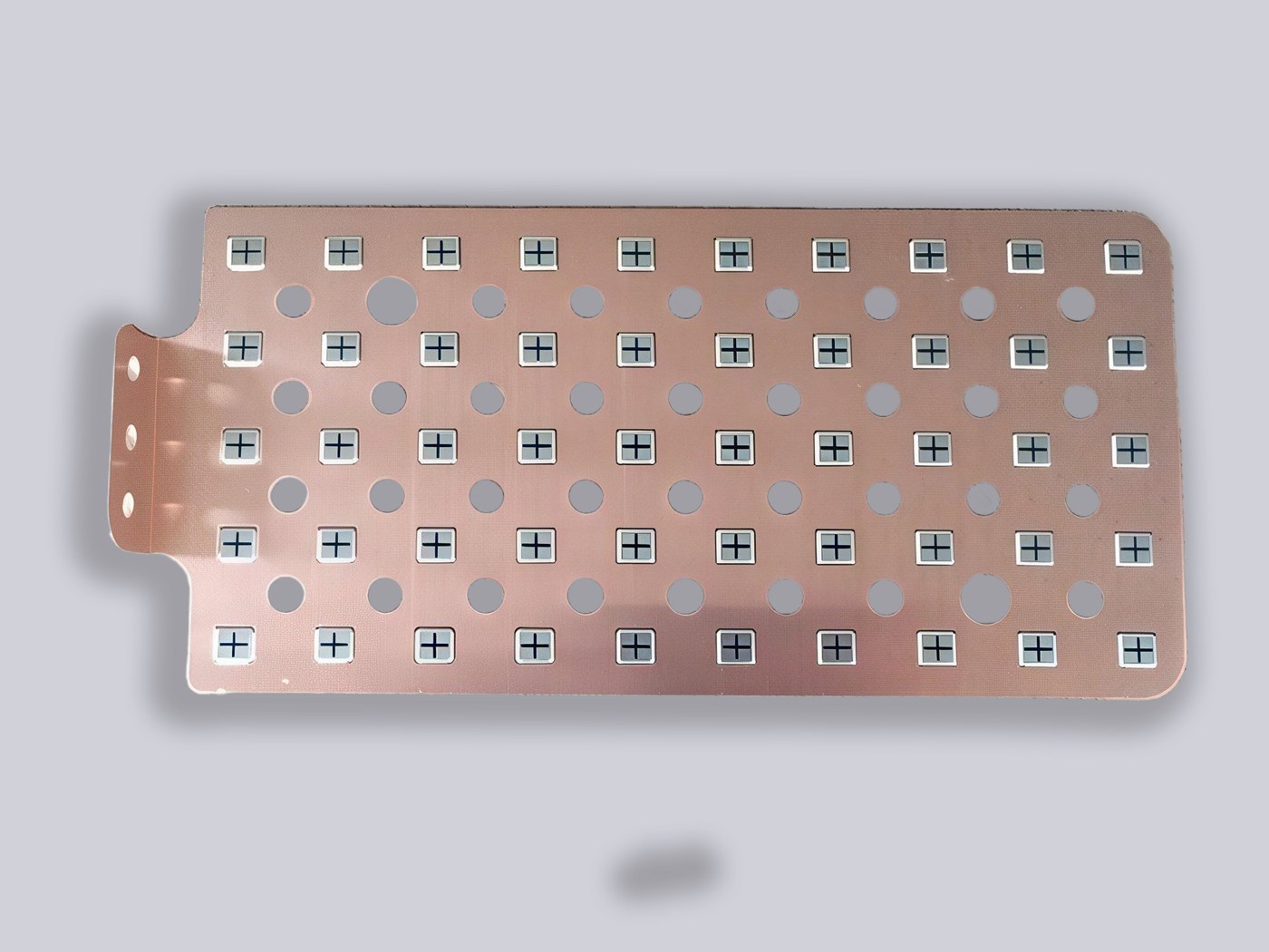
The inductance of a conductor depends on its shape and on the proximity of the opposite current path. The lowest-inductance geometry available is parallel planes, which is exactly what a laminated busbar is: flat positive and negative conductors separated by a thin dielectric. To minimize inductance, the conductors are brought extremely close together, in some designs to under 100 µm of insulation distance.
Same conductor section, 1 m length, 1 mm gap; the order-of-magnitude comparison is striking:
| Configuration | Loop inductance |
|---|---|
| Pair of round wires, 1 mm apart | ≈ 0.4 mH |
| Equivalent laminated busbar, same section, 1 mm gap | ≈ 50 nH |
| Same busbar with high-end insulation, 0.2 mm gap | below 20 nH |
Two physical effects shape the number at high frequency. The skin effect pushes alternating current toward the outer surface of each conductor, and the proximity effect pulls opposite-direction currents onto facing surfaces of the opposing planes. In a laminated busbar those effects work in your favor: the opposing planes use each other's fields, and magnetic flux largely cancels in the gap. Loose round wires have no such cancellation, which is the real reason the same cross-section drops from 0.4 mH to about 50 nH. The sub-100 µm spacing is the mechanism, not marketing: tightening the gap shrinks the loop area that the flux sees.
Below about 60–75 kW, compact power PCBs can integrate control and power on one board; above that, a power-electronics laminated busbar is the preferred DC-link interconnection, because it delivers the low loop inductance together with durability and vibration resistance. The target zone for serious power electronics is the nanohenry range, not the millihenry range.
In practice, the real busbar is never two perfect rectangles. Terminal windows, bolt holes and staggered layers break the plane overlap, and every break is a local rise in loop area. That is why the geometry work happens at the terminals first, not in the straight runs: a straight 50 mm of plane contributes little inductance, while a bent terminal with an open magnetic gap can eat half the budget. The same parallel-plane stacking that cancels flux also shares current between layers; see the ampacity chart for how layer count changes the rating. When you send us a switching-cell drawing, the terminal and capacitor interfaces are where we look first.
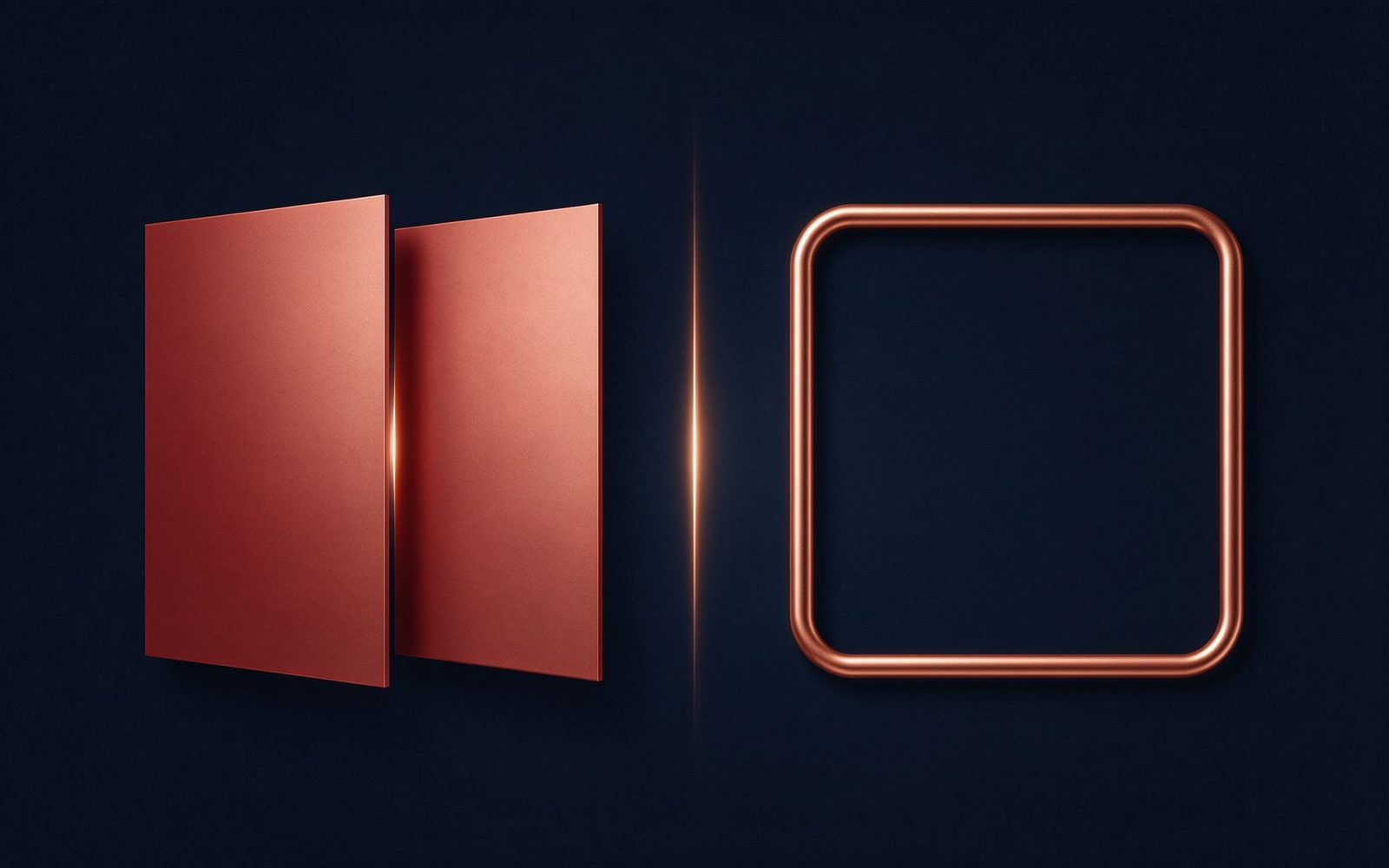
Stray inductance in the commutating circuit is influenced by the skin effect, mutual inductance, the length of the commutating path, the spacing between conductors, and the split structure of the busbar. Two empirical scaling rules are worth memorizing because they survive across geometries:
Spacing hurts far more than length, which is another way of saying: keep the opposing planes as close as possible. But because of layout asymmetry, component placement and the laminated structure, the commutating loop is almost always unbalanced.
Where does the imbalance come from? Layout asymmetry, component placement and the laminated stacking sequence all push current density around the loop, so one commutating path sees more inductance than another. The imbalance propagates into the main circuit, and the usual band-aids are extra snubber circuits and bigger heatsinks to suppress unbalanced voltage and thermal stress. Both are cost and size penalties you would not pay if the loop were balanced from the start.
The same imbalance logic applies when paralleling modules. If two switches in parallel see slightly different loop inductances, they share current unequally: the lower-inducting path carries more, heats more, ages faster, and sets the system rating. Balanced stacking and symmetric terminal placement are what let the paralleled devices actually share as planned. This is also why the busbar layout review cannot happen after the mechanical layout is frozen; the two are the same problem. Our practice is to treat loop balance as an explicit DFM variable: rearrange component placement, flip layer order, and check current sharing in simulation before the tooling stage.
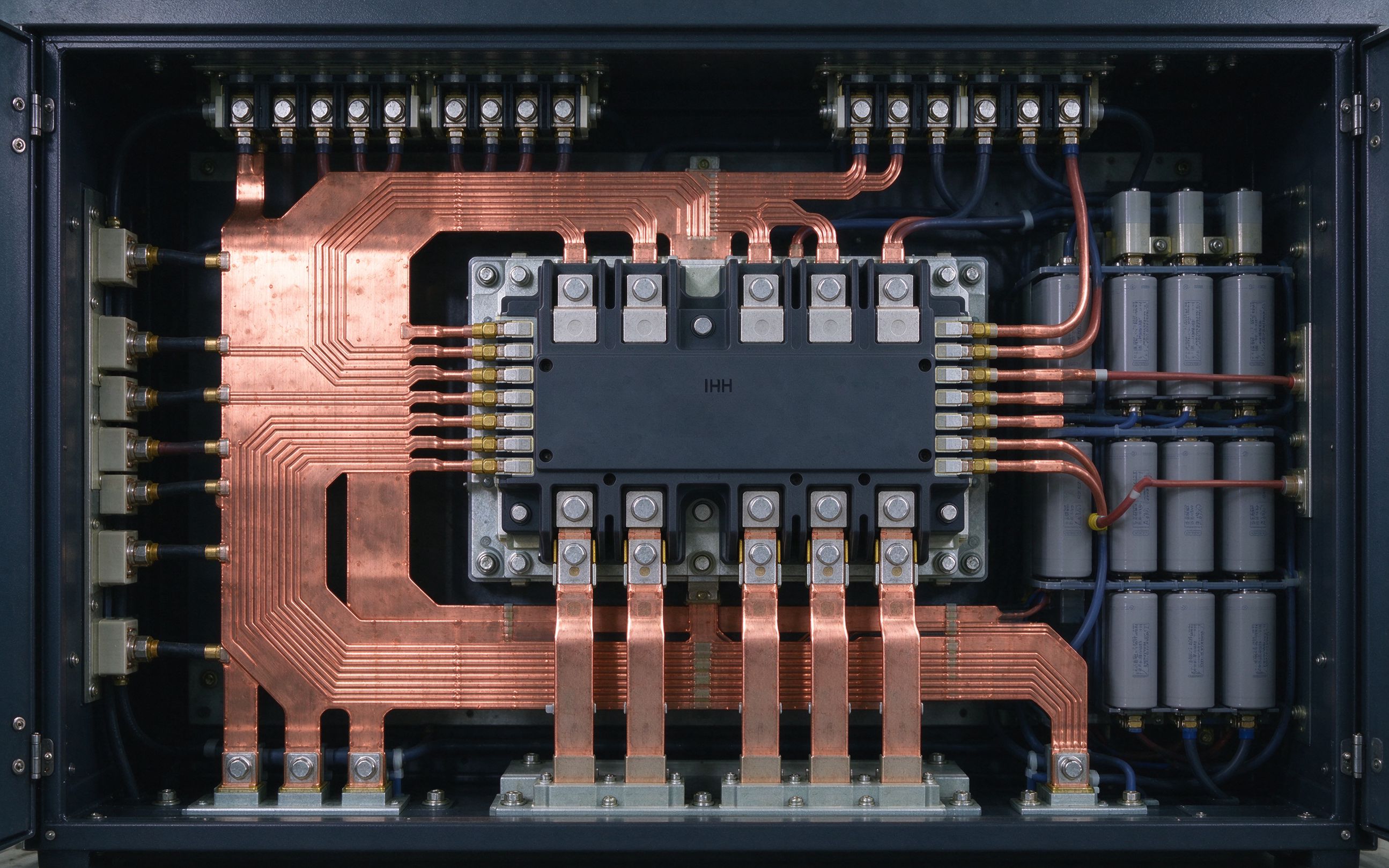
Measuring inductance on a physical prototype needs specialized lab equipment, delicate setup and at least one build, and small geometry changes move the number a lot, so an easily modifiable test sample is nearly impossible to construct. Finite element simulation needs no physical sample:
Two details matter. Replacing the capacitors with a short-circuit block forces the solver to follow the lowest-impedance path between the DC terminals, which is exactly the high-frequency commutating current path you care about. And sweeping frequency to MHz matters because magnetic flux is strongly frequency-dependent through skin and proximity effects; a solver run at one frequency gives you one number, while a sweep matched to your real switching slope gives you the number the device will actually see.
A typical optimization loop, example case at 5 kHz and a 1 A probe current, looks like this:
| Design step | Total loop inductance |
|---|---|
| Baseline, bent terminal, open gap | 12.0 nH |
| Flat terminal with connection bushings, smaller open gap | 9.2 nH |
| Increased overlap between terminals, flux cancellation | 4.5 nH |
Result: a 63% reduction with a fast iterative approach, ending below 5 nH. The biggest contributions came from the semiconductor connection terminal, the open-loop gap, and the capacitor connections. The lesson transfers to any commutation path: the biggest inductance lives at the interfaces, not in the bulk of the planes. Capacitor leads, bent terminals, and busbar-to-module bolts each open the loop; flat, overlapping, short interfaces close it again. Soldering DC-link capacitors directly onto the busbar is the most aggressive version of this, and it is the reason DC-link busbar assemblies with integrated capacitors exist.
Each rule has a failure mode behind it. An open magnetic gap at a terminal is a loop your current has to detour around; extra overlap cancels it. Thin insulation between planes shrinks the loop area, but below your PD design margin the part is no longer safe at voltage, which is why high-voltage designs get the partial-discharge margin checked in parallel. A compact layout cuts loop length, but packing the loop also traps heat, which is why we run the thermal check in thermal management at the same time. Balance matters because an unbalanced loop makes paralleled devices share current unequally, and the worst-paralleled device sets the rating.
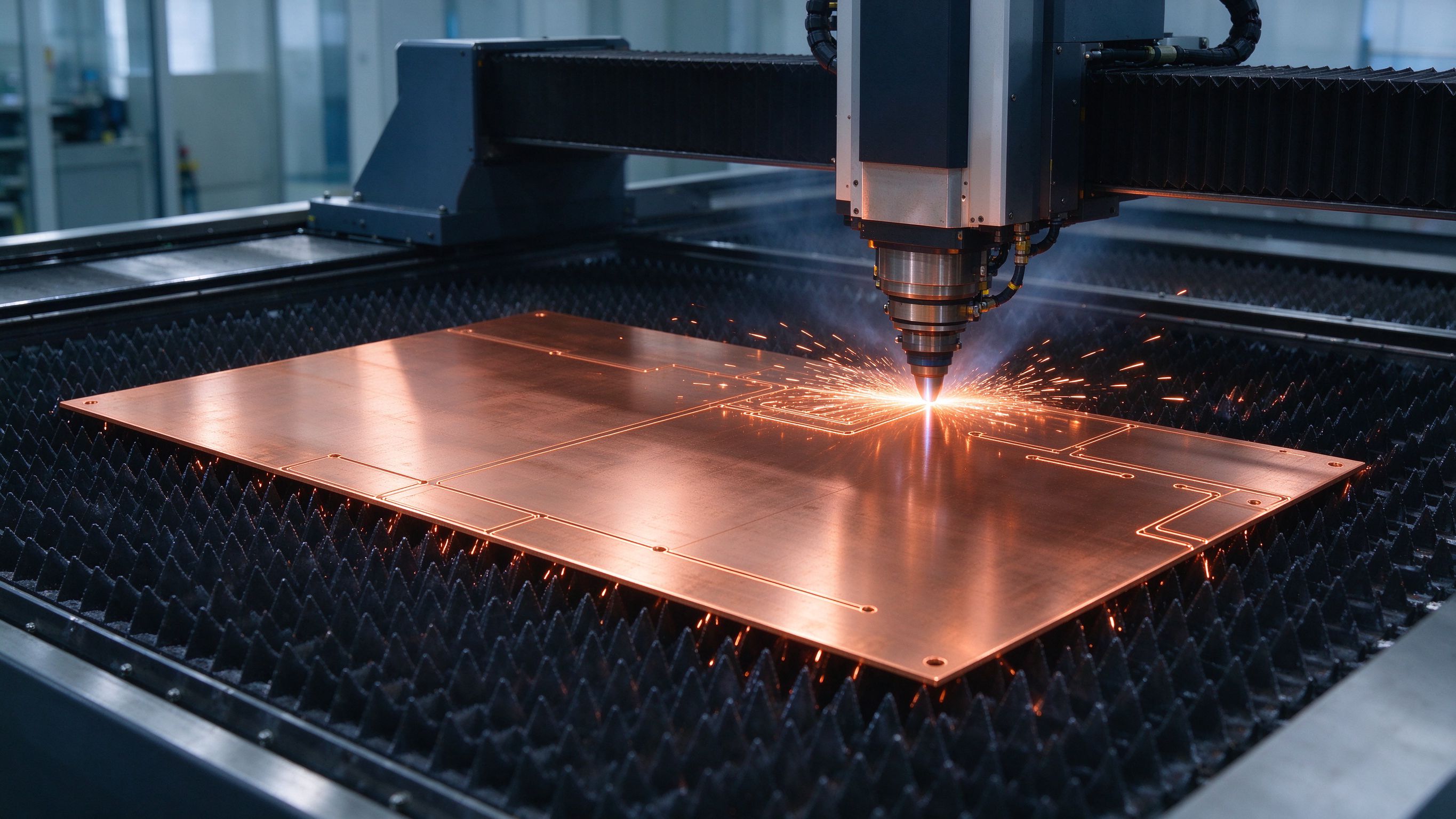
In traction inverters for battery EVs, stray inductance couples the electrical, magnetic and thermal problems together: it forces oversized design margins, blocks power-density gains, and affects component selection, ratings, switching frequency and temperature rise. In EV powertrain inverters and in industrial motor drives, that is exactly why the DC link is built as a laminated busbar rather than a wire harness. Compare the two approaches in our busbar vs cable harness guide.
Below about 60–75 kW, compact power PCBs integrate control and power stages on one board, and laminated busbars are not needed. Above that band, in traction inverters, DC/DC converters and the 100–500 A segment, the DC-link interconnection is where loop inductance becomes a product-spec parameter. The capacitor-integrated version of this architecture takes the rule capacitors-close-to-the-switches to its extreme: DC-link capacitors soldered directly onto the busbar instead of bolted on leads, which removes the last long bit of loop area from the circuit.
The other trend pushing this boundary is voltage. DC-bus voltages keep climbing toward 800 V and beyond in traction, which raises the di/dt available at the switch and shrinks the tolerance for every nanohenry in the loop. A DC link that was comfortable at 400 V deserves a second look at 800 V, even before the SiC upgrade.
When you send us a switching-cell drawing, with current, switching frequency, di/dt, and capacitor and semiconductor positions, we run the inductance and thermal review as part of DFM, before tooling. The numbers in this guide, 30% per doubled length, 80% per doubled gap, 50 nH versus 0.4 mH, are reference values from production-grade designs; treat them as the scale of the problem, not as your spec, and let the FEM loop close the last 10%. The starting checklist for any new program is in the design guide, or jump straight to contact engineering with your layout.
Send the current profile, voltage class and installation conditions — we will size the busbar and document the calculation with your quotation.
Send the current profile, voltage class and installation conditions — we will size the busbar and document the calculation.