Nidec Corporation, a global leader in motors and motion control, engaged SHANYUAN in 2025 to redesign the DC-link interconnection of a 1000 A servo-drive IGBT inverter platform produced in Japan and shipped worldwide. The delivered laminated busbar cut switching overshoot by 38%, reduced loop inductance to 6.8 nH and passed 3 kV partial-discharge testing — results verified in the customer's own test laboratory.
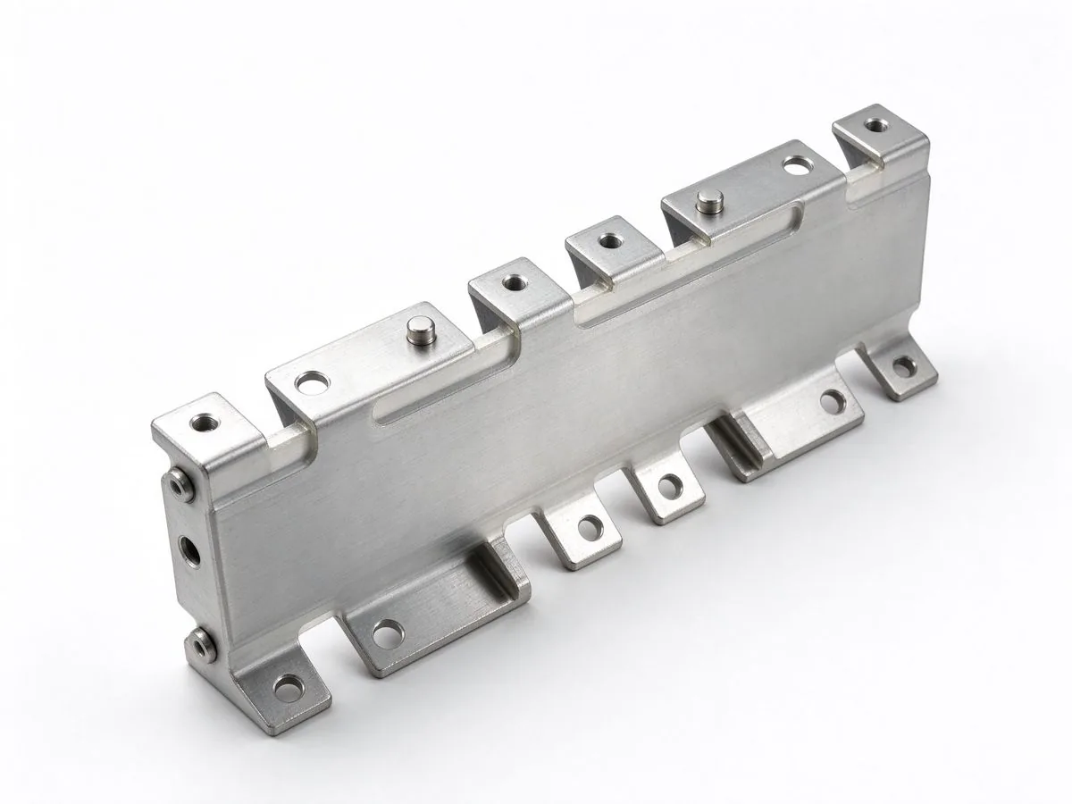
This case study is published as a representative engineering project. The product photograph and released drawing are illustrative of the delivered part; exact dimensions are covered by the customer's non-disclosure agreement.
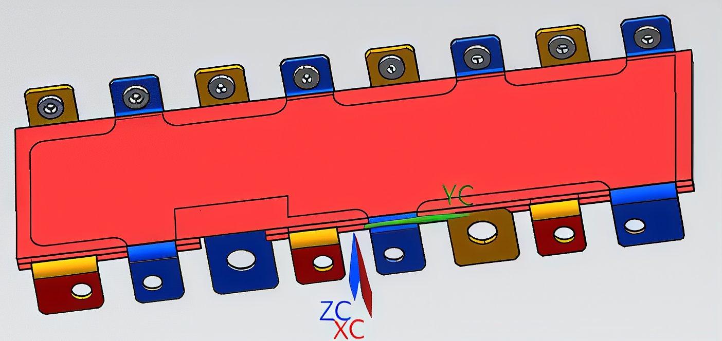
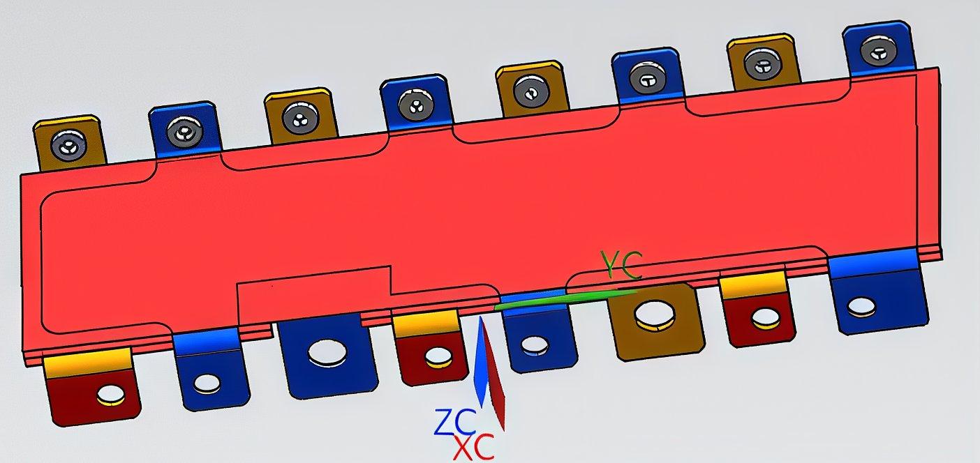
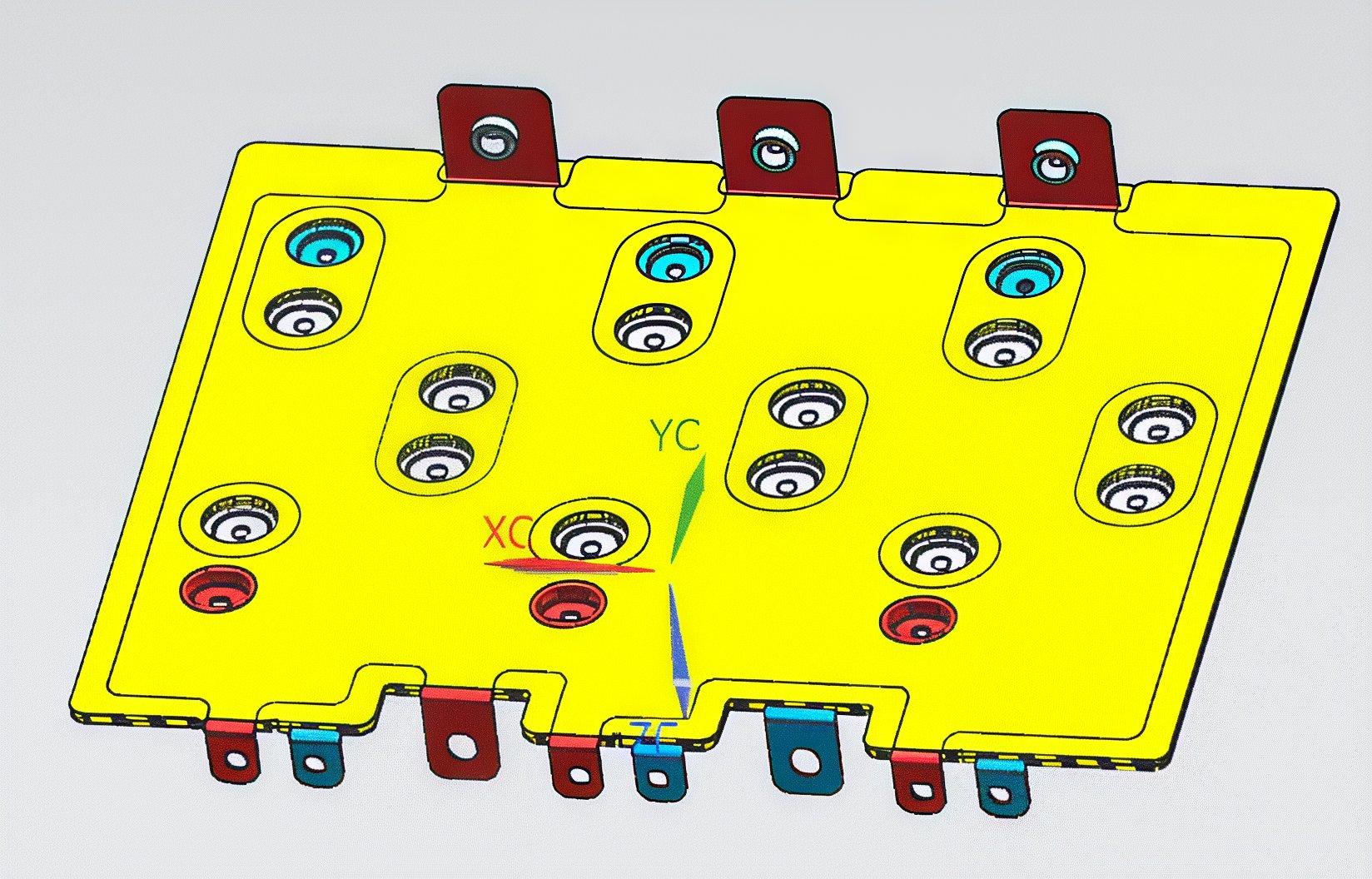
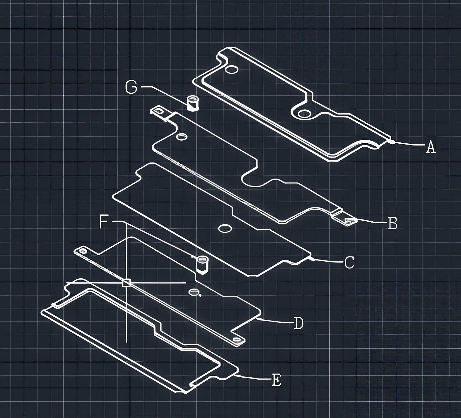
Customer drawings are treated as confidential; excerpts shown here are provided with permission and illustrate the layer stack, terminal layout and dielectric boundaries of the delivered part.
| Customer & platform | Nidec servo-drive IGBT inverter, 1000 A DC-link (Japan platform, global rollout) |
|---|---|
| Busbar type | 4-layer laminated DC-link busbar, C11000 copper conductors |
| Dielectric system | PET film + epoxy edge sealing, 3 kV DC withstand, PD-free to 1.6 kV |
| Loop inductance | 6.8 nH measured at module terminals (was 14.2 nH with cable assembly) |
| Current rating | 1000 A continuous at 70 °C ambient, 1500 A for 60 s overload |
| Temperature rise | ΔT 26 °C at rated current, hot spot on capacitor tabs |
| Terminals | M8 stud terminals for IGBT modules, blade terminals for film capacitors, tin-plated finish |
| Production | Tooling 5 weeks, 8-week PPAP sample cycle, 100% hi-pot and inductance scan per part |
| Quantified result | 38% lower switching overshoot, 6.8 nH loop inductance, 26 °C ΔT, 3 kV withstand |
Nidec Corporation, a global leader in motors and motion control, engaged SHANYUAN in 2025 to redesign the DC-link interconnection of a 1000 A servo-drive IGBT inverter platform produced in Japan and shipped worldwide. The delivered laminated busbar cut switching overshoot by 38%, reduced loop inductance to 6.8 nH and passed 3 kV partial-discharge testing — results verified in the customer's own test laboratory.
Nidec's motion-control division was qualifying a new servo-drive inverter platform around a 1200 V, 1000 A IGBT stack. The original DC-link used bolted copper cable assemblies between the capacitor bank and the power modules. On the test bench the design showed two problems: peak overshoot during hard switching reached 74 V above the DC bus, and the loop inductance budget was exceeded at high commutation currents.
The electrical team evaluated three options — re-routed cables, an aluminium-extrusion bus system and a laminated busbar. Cable re-routing did not meet the inductance budget, and the extruded system could not fit the platform's 22 mm clearance envelope. The engineering manager then approached SHANYUAN with the released mechanical drawings and asked for a power electronics laminated busbar that could be qualified within two quarters.
Our first step was a DFM review against the laminated busbar design guide: layer count, copper thickness, terminal layout and dielectric margins were confirmed with the customer's mechanical team before any tooling was cut.
SHANYUAN proposed a four-layer construction with interleaved positive and negative conductors, so that opposing current flow cancels loop flux in the inter-layer volume. C11000 copper conductors were stacked with 0.25 mm PET film, and all eight IGBT module connections were grouped on a single M8 stud rail to keep commutation loops short.
Loop inductance was simulated with a 3D field solver and cross-checked with an impedance analyser on prototype hardware. The measured 6.8 nH at the module terminals — 52% lower than the original cable assembly — came from the interleaved layer order plus a capacitor tab connection arranged so that the film-capacitor commutation loop overlaps the module loop. Layout guidance of this kind is documented in our low-inductance design resource.
Prototypes were shipped in week five of the project. The customer's power stage test bench measured the overshoot reduction directly: 74 V became 46 V, a 38% improvement, at the same dV/dt setting. The IGBT module busbar set format meant the part could be installed without any modification to the module footprint.
Conductor material is C11000 copper, tin-plated to 5 μm minimum, because the customer's environment includes condensation exposure during depot storage. Dielectric selection followed voltage class and temperature requirements: PET film rated for 3 kV DC withstand with epoxy edge sealing, giving a partial-discharge-free margin to 1.6 kV — verified with a 50 pC sensitivity PD tester.
The terminal set is deliberately standardised: M8 studs for the IGBT modules, blade terminals for film capacitors and a welded tab for the pre-charge circuit. All contact faces were machined flat within 0.05 mm and the bolt torque specification is 12 N·m ± 5%. Terminal engineering details — plating, torque, and joint resistance targets — are covered in the busbar terminal machining guide.
Creepage and clearance followed IEC 60664-1 for 1200 V pollution degree 2: a minimum 16 mm creepage across the epoxy edge and 8 mm clearance under the stud heads. The partial-discharge resource documents how these margins were derived from the PD test campaign.
Qualification followed the customer's PPAP plan with eight weeks of samples. Every part passed a 3 kV, 60 s hi-pot test, a 100% loop-inductance scan with a 100 kHz impedance bridge, and a thermal-rise test at 1000 A continuous in a 70 °C ambient chamber.
Temperature rise reached 26 °C at the capacitor tab hot spot, within the 30 °C limit. Thermal cycling — 500 cycles from −40 °C to +125 °C — produced no measurable change in joint resistance, and vibration testing followed IEC 61373 category 2 for the railway-grade qualification the platform later received. The quality and testing facility runs these tests in-house, which kept the whole qualification inside one supply chain.
Inductance, thermal and PD data were reported in a single test dossier per batch; the customer's quality team audited the production floor during sample phase and released the line for series production.
Series production runs in monthly batches of 600 parts, with a cycle time of 4.2 minutes per part across stamping, stacking, lamination and terminal assembly. The scrap rate in the first three months was 0.4%, driven by a pre-tooling DFM review that removed two bend-radius conflicts.
The customer's own bench test results, recorded in their test laboratory, confirm the quantified impact: loop inductance 6.8 nH (from 14.2 nH), overshoot 46 V (from 74 V), hot-spot ΔT 26 °C at rated current, and PD-free operation to 1.6 kV. Fewer wiring points also reduced the inverter's assembly time by roughly 11 minutes per unit — a benefit the customer attributed directly to replacing bolted cables with the laminated busbar.
Since qualification, the same busbar design has been quoted for two further Nidec platform derivatives. For engineers evaluating whether a laminated busbar fits their inverter, our inverter and UPS application page and the ampacity chart are the two starting points we recommend.
Higher switching speeds from SiC MOSFETs and modern IGBTs are pushing the DC-lin
Read article
SiC is scaling up — literally. Eight-inch wafer capacity is expanding at double-
Read article
Daniel Richter is the chief electrical engineer at SHANYUAN Laminated Busbars, with 15 years in laminated busbar design and current-carrying systems. He leads electrical dimensioning, DC-link layout and thermal simulation for power converters, EV platforms and HVDC stations, and holds an M.Sc. in El
Send the current profile, voltage class and terminal types — our engineers reply within one business day.