Partial discharge is the failure mode that never announces itself at the factory door. A laminate can pass hipot, carry load for years, and still be quietly eroding from the inside because a microscopic void sits where the electric field is highest. At 1 kV this is a nuisance; at 10 kV and above it is a reliability cliff. This guide explains how partial discharge starts inside a laminated busbar, what design measures keep it out - field grading, void-free lamination, edge and termination control - and which test numbers actually prove PD-free operation. The principles come from work on high-voltage planar bus structures: a 16 kV-rated, PCB-based DC bus was demonstrated PD-free to 18 kV, and an optimised laminate bus for a 10 kV SiC module reached a partial discharge inception voltage of 11.6 kV rms (CPES Virginia Tech, 2020-2021).
Partial discharge is the failure mode that never announces itself at the factory door. A laminate can pass hipot, carry load for years, and still be quietly eroding from the inside because a microscopic void sits where the electric field is highest. At 1 kV this is a nuisance; at 10 kV and above it is a reliability cliff. This guide explains how partial discharge starts inside a laminated busbar, what design measures keep it out - field grading, void-free lamination, edge and termination control - and which test numbers actually prove PD-free operation. The principles come from work on high-voltage planar bus structures: a 16 kV-rated, PCB-based DC bus was demonstrated PD-free to 18 kV, and an optimised laminate bus for a 10 kV SiC module reached a partial discharge inception voltage of 11.6 kV rms (CPES Virginia Tech, 2020-2021).
Partial discharge (PD) is a localised electrical breakdown that does not bridge the full insulation gap. It happens in voids, at conductor edges, or on surfaces where the local field exceeds the material's withstand - and it deposits energy into the insulation on every cycle. Over months and years, that repeated erosion turns a sound dielectric into a tracked, conductive failure path.
PD is measured in picocoulombs (pC). The industry rule of thumb for solid insulation: inception should be suppressed below 10 pC at the rated operating voltage, and for medium-voltage duty, modern specifications commonly demand <10 pC at rated voltage (busbar insulator practice, 2026).
Laminated busbars are built by stacking copper layers and dielectric films, then bonding under heat and pressure. The voids that matter are born in three places: trapped air between film layers during lay-up, solvent or moisture outgassing during the bonding cycle, and micro-gaps at the film edge where lamination pressure is lower.
Vacuum-assisted lamination exists precisely to kill the first two. When the stack is bonded under vacuum, air has nowhere to hide, and the result is a denser, void-free interface. That is why high-voltage bus structures for MV converters use vacuum lamination as a non-negotiable process step (CPES Virginia Tech, 2020).
Air has a breakdown strength around 3 kV/mm at atmospheric pressure, an order of magnitude below the 15-30 kV/mm that PET, Nomex and epoxy insulation carry. A void is therefore a hole in the dielectric armour: the field concentrates across it, the air breaks down first, and the discharge slowly eats the surrounding material.
Because the void is small, the breakdown is partial - it does not trip the hipot - but it is persistent. This is why two laminates with identical dielectric stacks can have completely different service lives: one is void-free, the other is not, and only PD testing tells them apart.
PD does not start at the highest voltage - it starts at the highest field concentration. In a planar bus, the field crowds at conductor edges, at plated and non-plated through-holes, and at surface-mount pads (CPES Virginia Tech, 2020). Field grading moves that peak away from air and into the dielectric, where the breakdown strength is higher.
The practical toolbox: embedding conductors in internal layers, shielding layers that shift the peak E-field to a controlled plane, and grading plates or patterns that shape the equipotential distribution at edges. In one 10 kV module design, copper traces inside the PCB were used as field-grading plates to shift the peak field from air into FR4, achieving PD-free operation at 11.6 kV rms (CPES Virginia Tech, 2021).
The highest-risk geometry in any busbar is the triple point - where conductor, insulation and a third medium (usually air or potting) meet. At a terminal, the field can concentrate at the junction of metal, film and air, and surface discharge starts there long before the bulk insulation is stressed.
Three countermeasures dominate: shield the triple point with a conductive or semi-conductive layer so the peak moves into the insulation; lengthen the creepage path with film extension or sleeves; and avoid sharp metal edges at the termination. The second and third are pure geometry; the first needs a design decision early, because a shielding layer changes the whole stack-up.
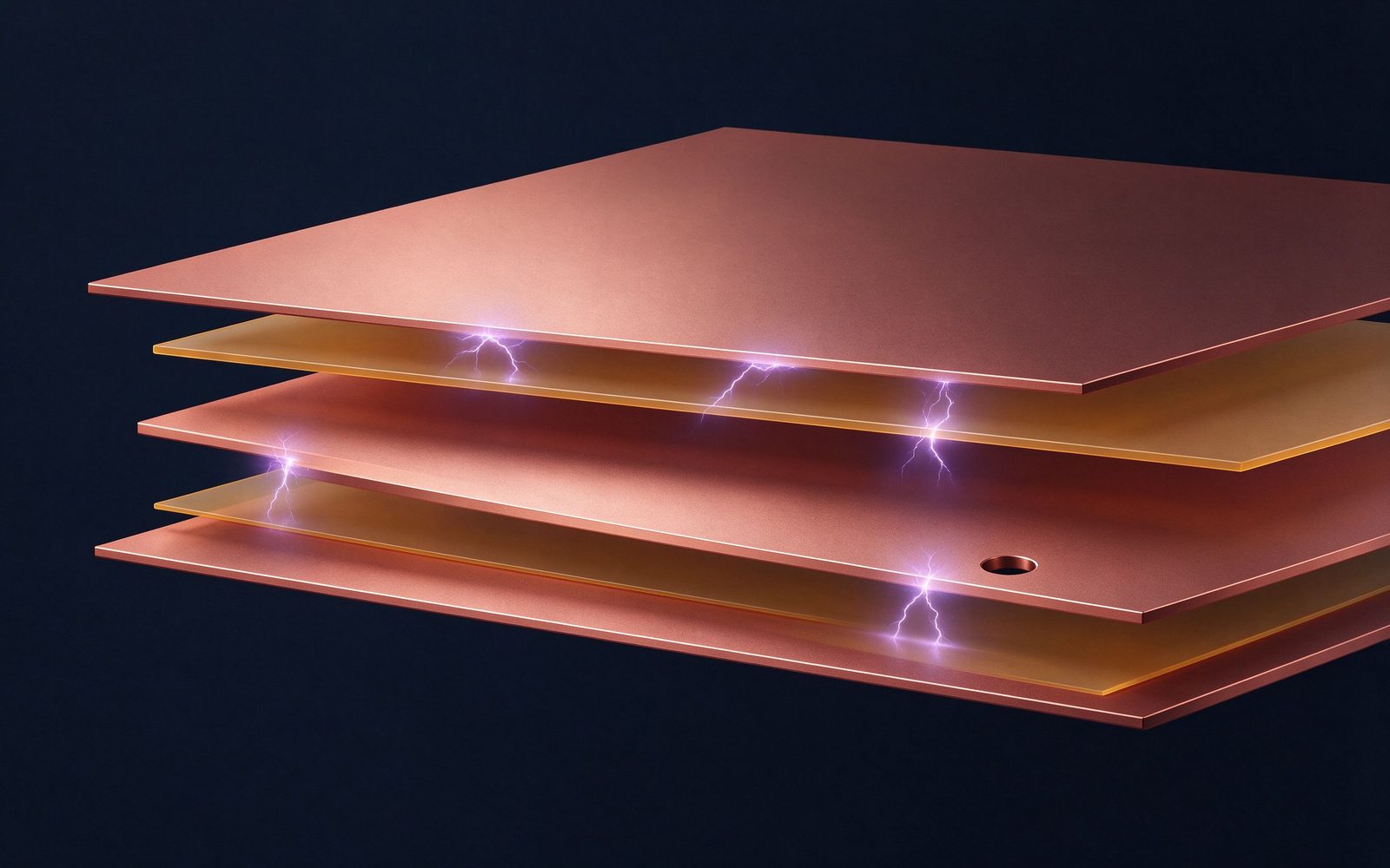
Field enhancement at a sharp corner scales roughly with the radius: a knife-edge concentrates field to many times the average stress, a rounded edge brings it down dramatically. In laminate design, the conductor's edge profile is set at the stamping stage and cannot be fixed later by the insulation.
Practical guidance: specify a minimum edge radius on the copper before quoting, and check the drawing for stamping burrs - a burr is a built-in PD source. For high-voltage duty, consider film edge extension beyond the conductor edge, so the dielectric, not the air, takes the stress at the boundary.
PD testing under DC stress behaves differently from AC. Under AC, a void discharges twice per cycle; under DC, the discharge repetition rate depends on charge relaxation in the void - often much lower, which makes DC PD harder to detect and easier to underestimate.
Converter and ESS DC-link busbars therefore need DC PD testing specifically, not just the AC test inherited from distribution practice. A 16 kV-rated planar bus was demonstrated PD-free to 18 kV DC with a measured PDIV of 20 kV between the DC poles (CPES Virginia Tech, 2020) - the DC test being the relevant one for inverter duty.
Two numbers matter on the test sheet. PDIV - partial discharge inception voltage - is the voltage where discharge first appears as voltage rises. PDEV - partial discharge extinction voltage - is where it stops as voltage falls. The gap between them is hysteresis: a material that starts discharging at 8 kV may keep discharging down to 5 kV, and extinction matters for systems that see voltage dips.
When you spec a busbar, ask for both, tested per IEC 60270 with the background noise floor stated. A vendor that quotes only PDIV is telling you half the story.
The <10 pC target at rated voltage is a practical threshold, not a magic number - it separates genuine insulation integrity from a void-laden stack that will fail in service. The measurement chain is standard: coupling capacitor, calibrated to a known charge, with the test object stressed at rated voltage and above.
For a busbar programme, the acceptance test typically runs: ramp to PDIV and record; hold at rated voltage and verify <10 pC; ramp down and record PDEV. Sample testing is fine for production, but the design qualification should be on representative parts with the same tooling and materials as production.
PD at the surface follows creepage distance and clearance just as much as bulk insulation does. Contamination, humidity and altitude all shorten the effective creepage path, and PD on a dirty surface quickly becomes tracking - a carbonised conductive trail that ends in flashover.
Our creepage and clearance design guidance covers the dimensioning rules; the PD angle is the verification: surface PD testing under the expected environmental condition (humidity, or a pollution class) rather than a pristine lab environment. For outdoor or partially enclosed busbars, the difference is material.
PET film is the workhorse: high dielectric strength (typically >200 V/µm), low cost, clean lamination. Nomex adds thermal margin and mechanical toughness, which matters for higher temperature classes and cycling duty. DLF (double-layer film) and other laminates trade cost against PD margin in the same way.
The material choice sets the ceiling; the process sets whether you reach it. A mediocre film stack, laminated void-free, will outlive a premium film stack with voids. That is why process control - not just the material spec - is the real PD decision.
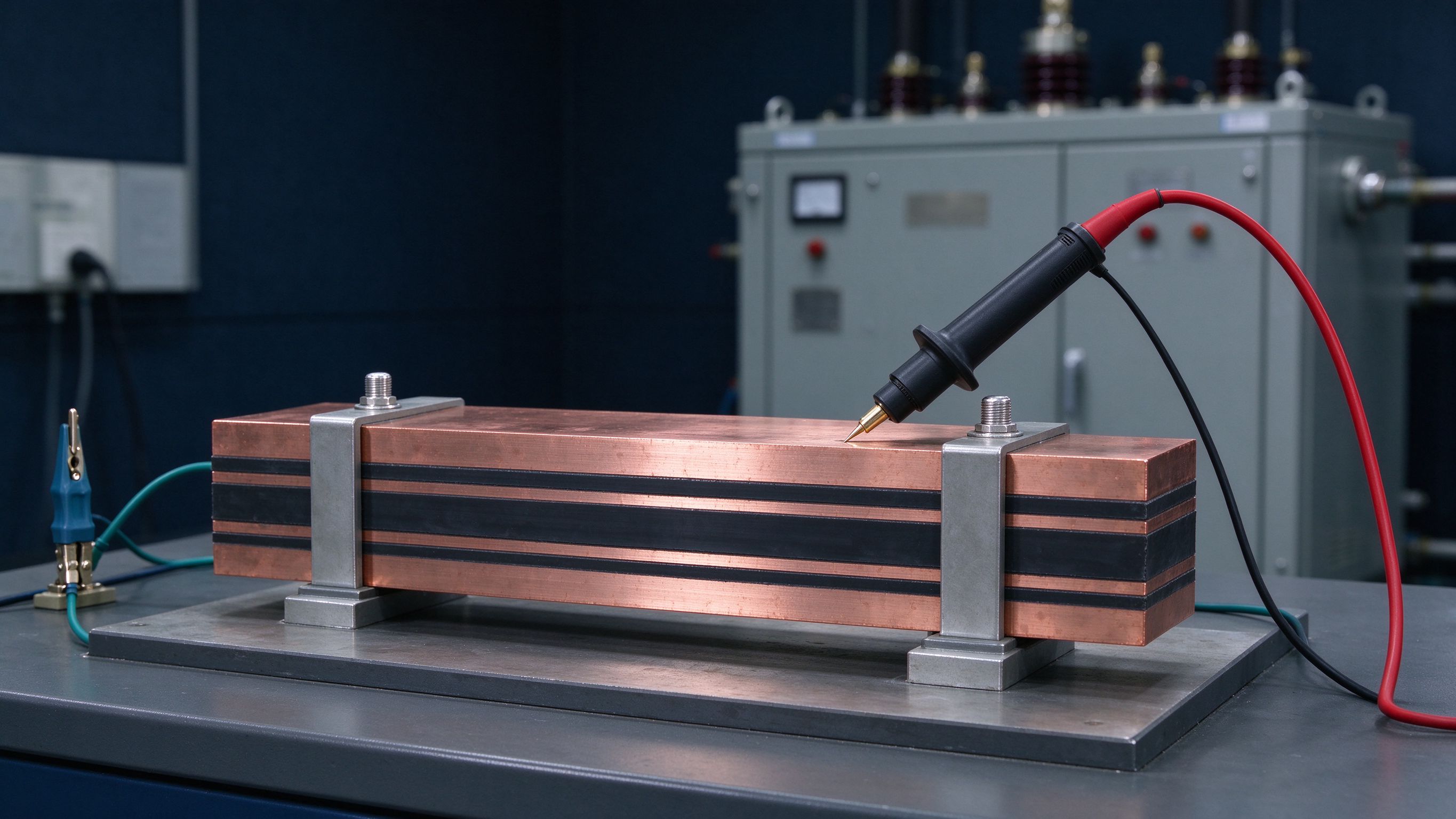
When you put a high-voltage busbar on the market or into a production programme, the PD requirement belongs in the specification, not in a later conversation. Minimum three items: PDIV and PDEV targets per IEC 60270, a <10 pC limit at rated voltage, and the test method stated (AC and/or DC depending on duty).
Add the process expectations - void-free lamination, edge radius, shielding if required - and the documentation: PD test reports per design qualification, plus sample records from production. That file is what separates a busbar that ships from a busbar that performs.
SHANYUAN produces laminated busbars with void-controlled lamination and per-lot dielectric testing, including hipot, insulation resistance and continuity records with CoC. For higher-voltage programmes we qualify the stack - layer count, film type, edge extension - against the PD targets before production tooling is cut.
Send the voltage class, dielectric requirements and test limits with your drawing; our engineering team will confirm the stack and the qualification plan, and reply within one business day.
PD testing is slower and more expensive than hipot, so production screening is usually sample-based - a defined frequency, for example one part per lot or per shift, run through the full PDIV/PDEV sequence while every part gets the routine hipot. The sample record then anchors the lot.
The trap is drifting process: a tooling change, a new film batch or a lamination temperature shift can reintroduce voids without tripping routine tests. The fix is a control chart on the sample PDIV - if the inception voltage creeps down across lots, the process moved and the investigation starts before the field failure, not after.
A PD-free busbar can be defeated after it leaves the press. Handling scratches the insulation; assembly tools nick the film at the terminations; and a screw driven too deep at a mounting point becomes a local stress concentration. The design phase should assume some abuse and build margin for it: thicker film at handling zones, protective edge covers, and clear assembly instructions on torque and tooling.
For high-voltage programmes, our drawings specify the handling and assembly constraints on the same sheet as the electrical requirements - because the part that arrives PD-free is only useful if it is still PD-free after installation.
Not every busbar needs PD-free design. Below roughly 1 kV, void-related PD is rarely the life-limiting mechanism - thermal and mechanical issues dominate. The case for PD-free specification strengthens above 1 kV, and becomes non-negotiable at 3.3 kV and up, in converter and MV duty, and wherever the insulation is thin relative to the voltage class.
The decision rule for a buyer: if the system voltage is above 1 kV, or the duty is converter-fed DC (which sees switching transients), put PDIV/PDEV and the 10 pC limit in the spec. Below that, the cost of PD testing may not buy anything meaningful.
PD testing adds cost - equipment, time, engineering review - and the budget question is legitimate. The failure it prevents is rarely spectacular: not a hipot trip at the factory, but a mid-life dielectric breakdown in the field, a warranty claim, a downtime event, and a root-cause investigation that ends at the void nobody tested for.
For a production programme the cost comparison is stark: sample PD testing adds a small percentage to unit cost, while a field failure on a converter or ESS rack costs orders of magnitude more. The specification decision is a risk decision, and the risk is asymmetric in favour of testing wherever the voltage justifies it.
A PD test report is only useful if you can read it. The essentials: test circuit and calibration (per IEC 60270), background noise floor, PDIV with the ramp rate, the magnitude at rated voltage in pC, PDEV on the way down, and the environmental conditions (temperature, humidity, altitude).
Two red flags: a noise floor close to the 10 pC limit, which makes the pass meaningless, and a report that quotes only PDIV without PDEV. If a supplier's report lacks either, ask for the full test record - the answer tells you whether the test was real.
Above 1,000 m, air density drops and so does its breakdown strength - roughly 1% per 100 m in some guidance. A PD margin set at sea level can silently shrink on a high-altitude site, and surface discharge at thin air starts earlier than the factory test predicted.
For high-voltage busbars installed in plateau regions, either derate the operating voltage, thicken the dielectric, or extend creepage per the altitude correction. The PDIV/PDEV figures in the test report are measured at the test altitude; the installation altitude needs its own check, not an assumption.
DC-link busbars in converter duty see more than DC stress: they see the switching transients of the devices beside them. Each switching event puts a dv/dt step on the bus insulation, and if a void is present, the fast edge can initiate discharge that the steady DC field alone would not start. This is why PD-free design is not optional for converter-fed buses at medium voltage.
The design response is the same toolbox - voids out, field graded, edges radiused - applied with the transient in mind. If the system's dv/dt is high, ask for the PD test under the converter's waveform, or at least under DC, rather than a pure 50 Hz AC test.
Insulation testing answers four questions: does it withstand rated voltage, does it discha
Read articleA busbar fails across a surface long before it fails through its insulation if the creepag
Read article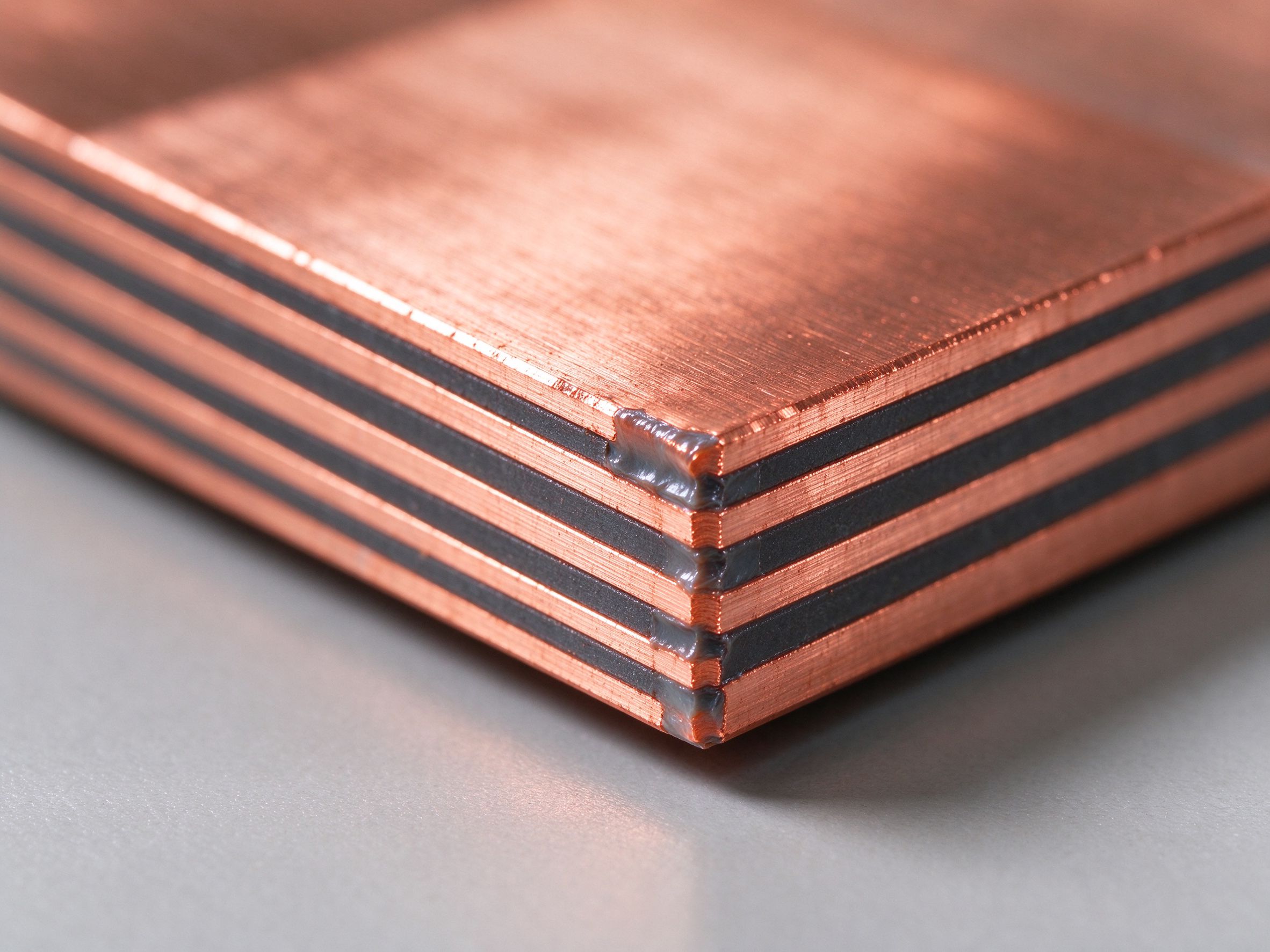
PET, Nomex and DLF epoxy are the three dielectrics we laminate into SHANYUAN busbars every
Read articleSend the current profile, voltage class and terminal types — our engineers reply within one business day.