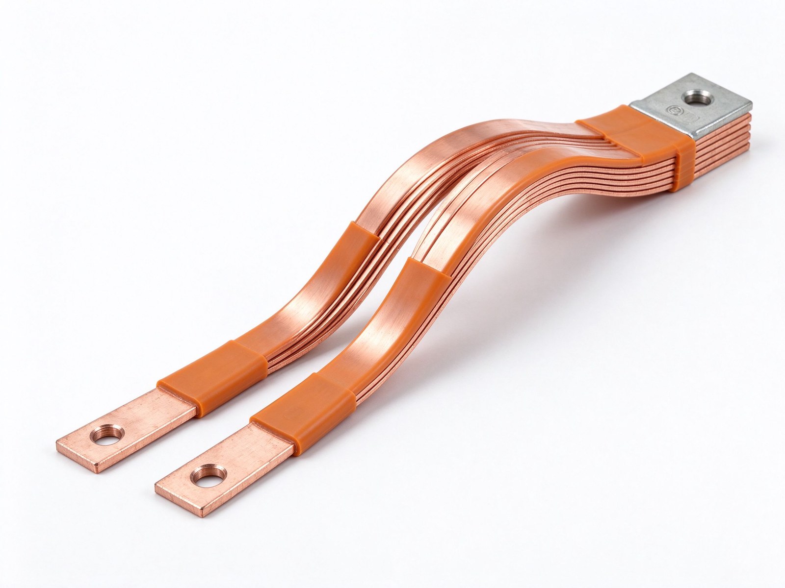
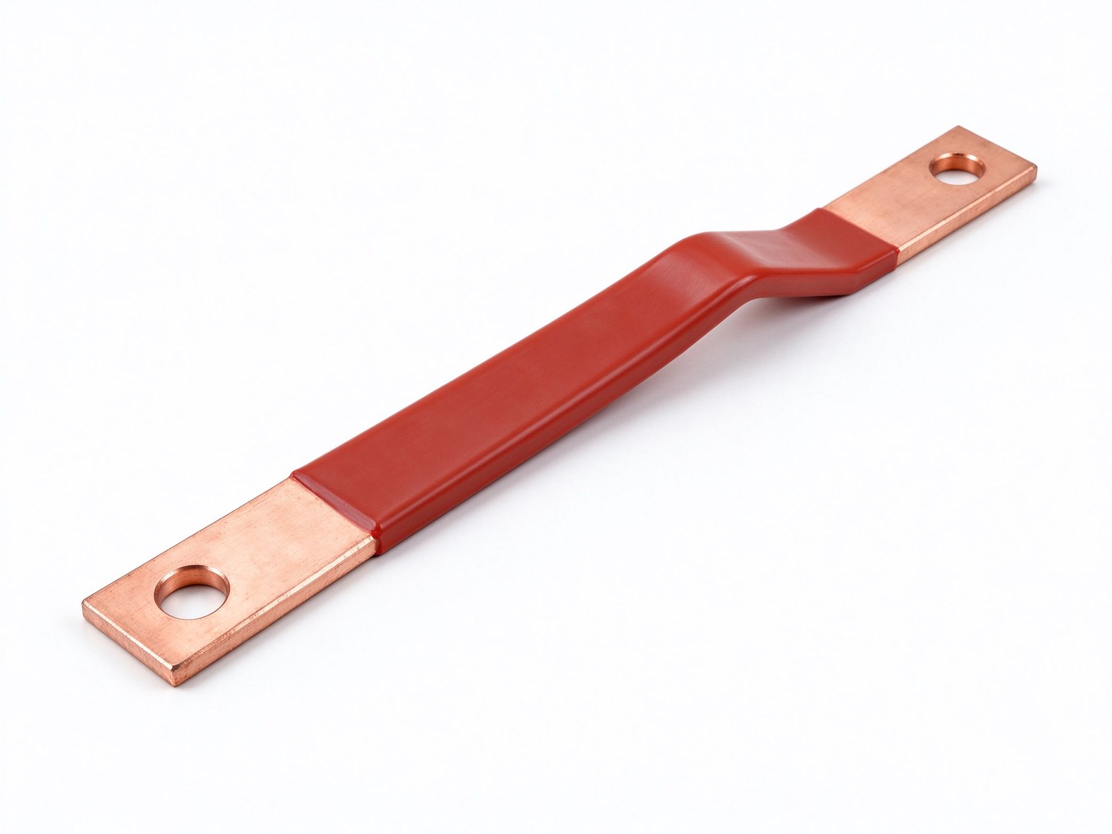
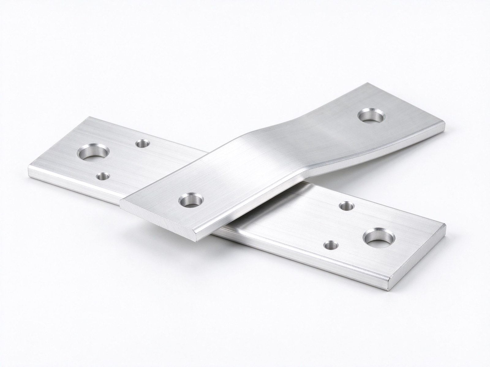
Multi-layer laminated copper busbar with thin dielectric films for low-inductance power distribution.
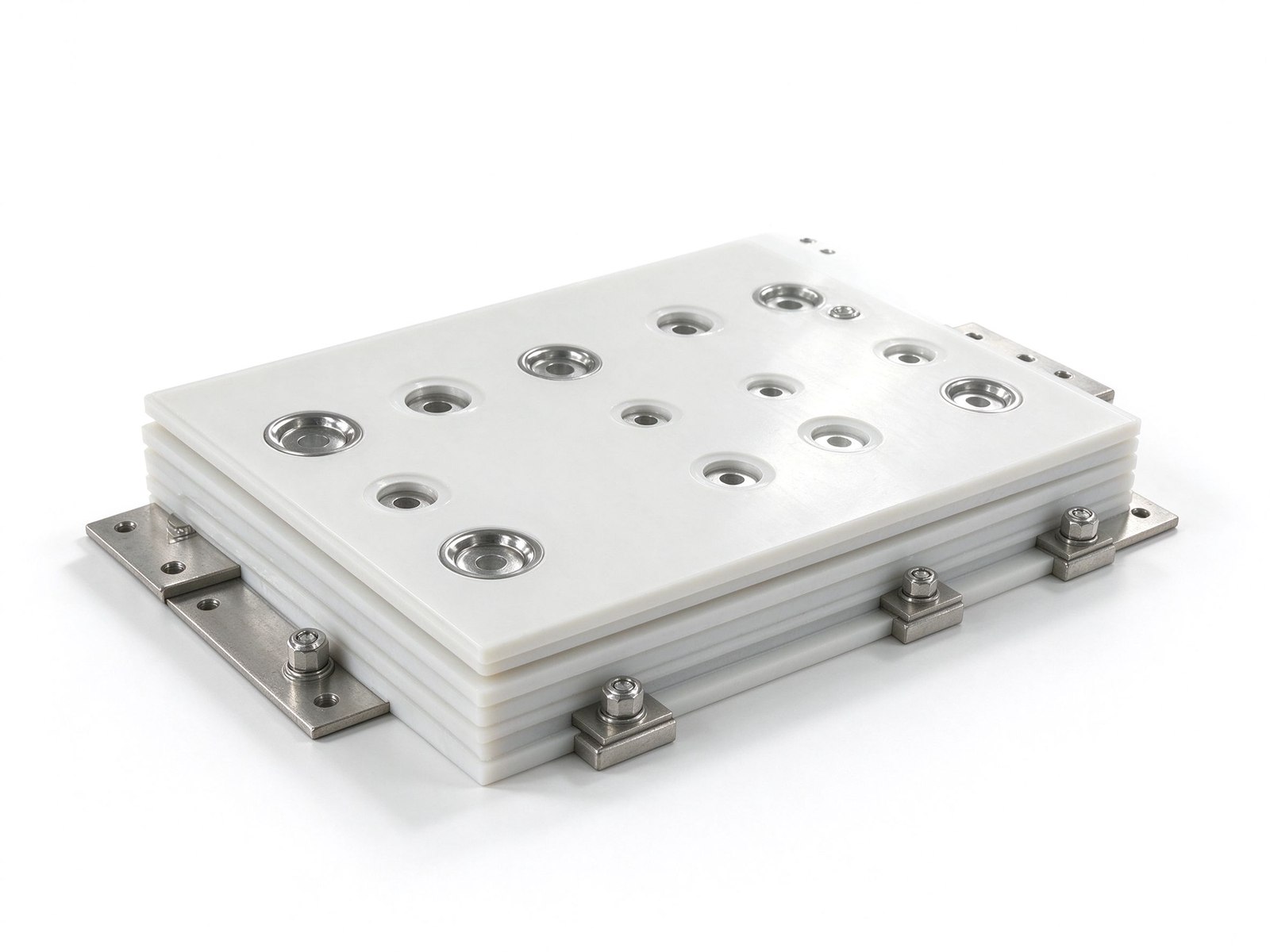
Product imagery: factory photo plus studio renders. The exact geometry, layers and terminals of your part follow your drawing.
Final values follow your drawing — this is the standard configuration of the family.
| Parameter | Value |
|---|---|
| Conductor | C11000 copper, tin plated |
| Conductor layers | 2–6+ per stack |
| Dielectric spacing | 5–10 mil (0.13–0.25 mm) typical |
| Dielectrics | PET, Nomex, PEN, FR4, Kapton (per voltage class) |
| Integrated cooling | Aluminium liquid-cooling layer optional |
| Current rating | Per design, up to ~1000 A |
| SKU | SY-CM-301 |
Key characteristics of this product family.
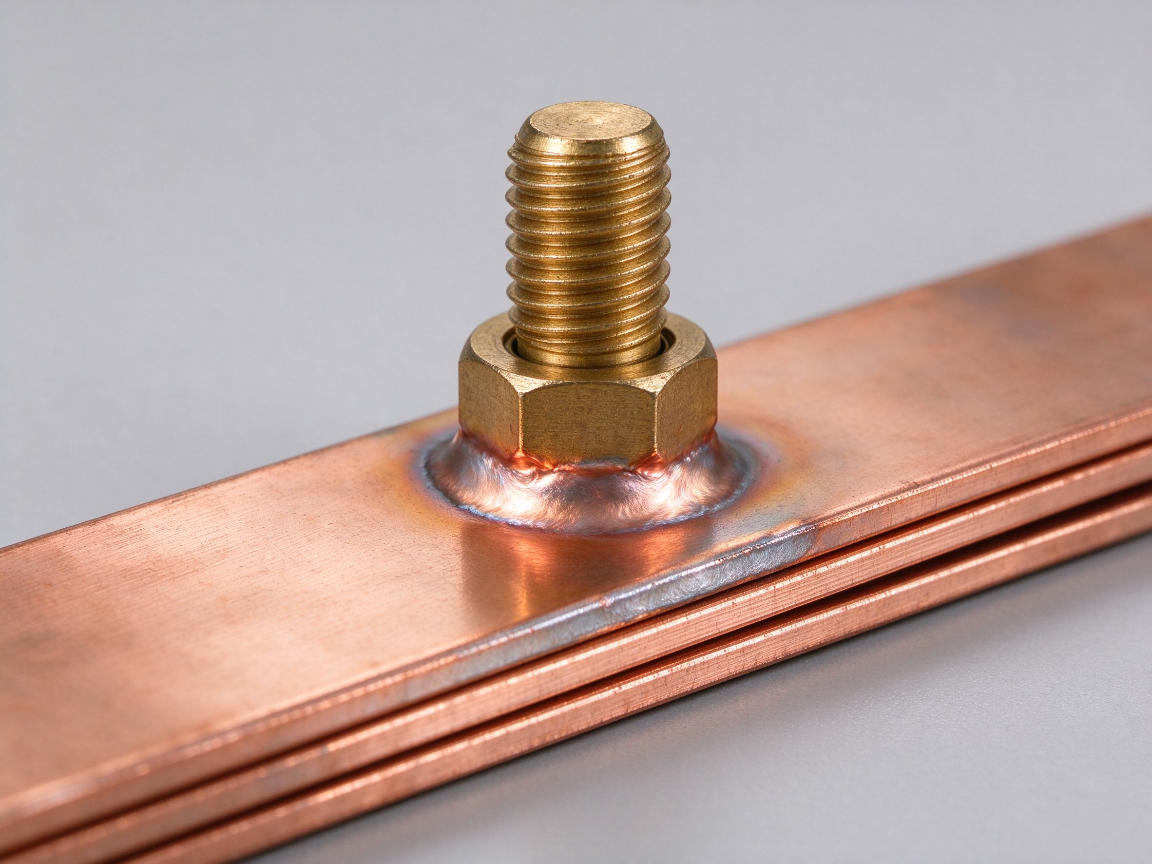
A laminated busbar is built by stacking multiple copper conductor layers with thin dielectric films between them and bonding the stack under heat and pressure into one integrated part. Because adjacent layers carry current in opposite directions, the magnetic fields cancel and stray inductance drops sharply — the key benefit for fast-switching IGBT and SiC circuits. The assembly can also integrate an aluminium cooling layer with internal channels, turning the busbar itself into a liquid-cooled heatsink for high-density converters.
Where this busbar configuration earns its place.
Where this busbar configuration earns its place.
Where this busbar configuration earns its place.
Where this busbar configuration earns its place.
Where this busbar configuration earns its place.
Where this busbar configuration earns its place.
Your drawings reach the engineers who build the part.
Design risks flagged when changes are cheap.
Test records per lot, CoC and PPAP on request.
Drawing to delivered production parts, one supplier.
From spec review to shipped, tested parts — one accountable supplier.
Straight answers from the engineering team.
Every SHANYUAN busbar is custom, but the power circuits they connect recur across markets. Three typical ones — send us yours and we will point to the right stack-up.
Tight, low-inductance links between the battery source and traction inverters, fully edge-sealed for 400–800 V platforms.
ExploreCommutation-loop connections from DC-link capacitors to IGBT bridges, designed against switching overshoot V = L × di/dt.
ExploreConverter DC links built for rising bus voltages toward 1500 VDC, with creepage and partial-discharge margins included.
ExploreLayers, terminals, dielectrics and mounting are all configurable. Send us your spec for DFM review and a quotation within one business day.
Send drawings, current ratings and voltage class — DFM feedback and a quotation within one business day.