Buyers often ask for 'the most layers we can get' — which is the wrong question. Laminated busbar layer count is a design variable traded against inductance, dielectric stress, thermal path and price. This article gives purchasing managers and engineers a decision framework they can apply before the RFQ goes out.
Buyers often ask for 'the most layers we can get' — which is the wrong question. Laminated busbar layer count is a design variable traded against inductance, dielectric stress, thermal path and price. This article gives purchasing managers and engineers a decision framework they can apply before the RFQ goes out.
A laminated busbar sandwiches copper conductors between thin dielectric layers. The layer count is the number of copper planes in the stack. A 2-layer assembly carries two conductors (typically a positive/negative or phase/neutral pair); a 4-layer stack might carry two DC pairs, a 3-phase plus neutral, or split planes for EMI control; a 6-layer stack is usually two independent 3-layer zones or a complex mixed DC/AC path.
Adding layers buys four things: lower stray inductance per ampere, tighter packaging, built-in EMI screening between planes, and fewer separate busbar runs. It costs three things: more dielectric area to fail, a thicker stack that is harder to bend and support, and more manufacturing complexity — hence more price. The skill is knowing which side of that trade your application sits on.
The dominant reason to laminate at all is stray inductance. In a conventional cable pair, the current loop area is large and the stray inductance sits in the hundreds of nanohenries. A 2-layer laminated pair puts the forward and return conductors face-to-face across a 0.1-0.5 mm dielectric, collapsing the loop area; measured values on production parts typically land in the 5-20 nH range at 1 m length (IEEE 1341 methodology).

A 4-layer stack can reduce net loop inductance further and, more importantly, cancels differential-mode fields by pairing each conductor with its return. If your converter is switching IGBT or SiC modules at high di/dt, the loop inductance measurement guide on this site explains how to verify the spec rather than trust the drawing. The measurement method matters — a two-terminal measurement on a bare bar reads different numbers than a loop measurement through the connected module.
Voltage class sets a floor on the dielectric system, not on layer count. At 800V-1.5 kV DC links, a single PET layer (typically 0.25-0.5 mm) with adequate clearance is common; at 3.3-4.5 kV, the insulation needs either thicker PET, Nomex, or DLF film, and creepage distances start to dominate the layout. Our dielectric selection guide covers film choice in depth.
The interaction with layer count is practical: every additional plane adds another dielectric interface that must withstand the same system voltage, and stacked interfaces need the same partial-discharge-free quality as the first one. A 6-layer assembly for a 4 kV link has six chances for a PD defect — which is why PD testing becomes a per-layer, not per-assembly, discipline. The PD-free design article lists the design rules that keep those interfaces clean.
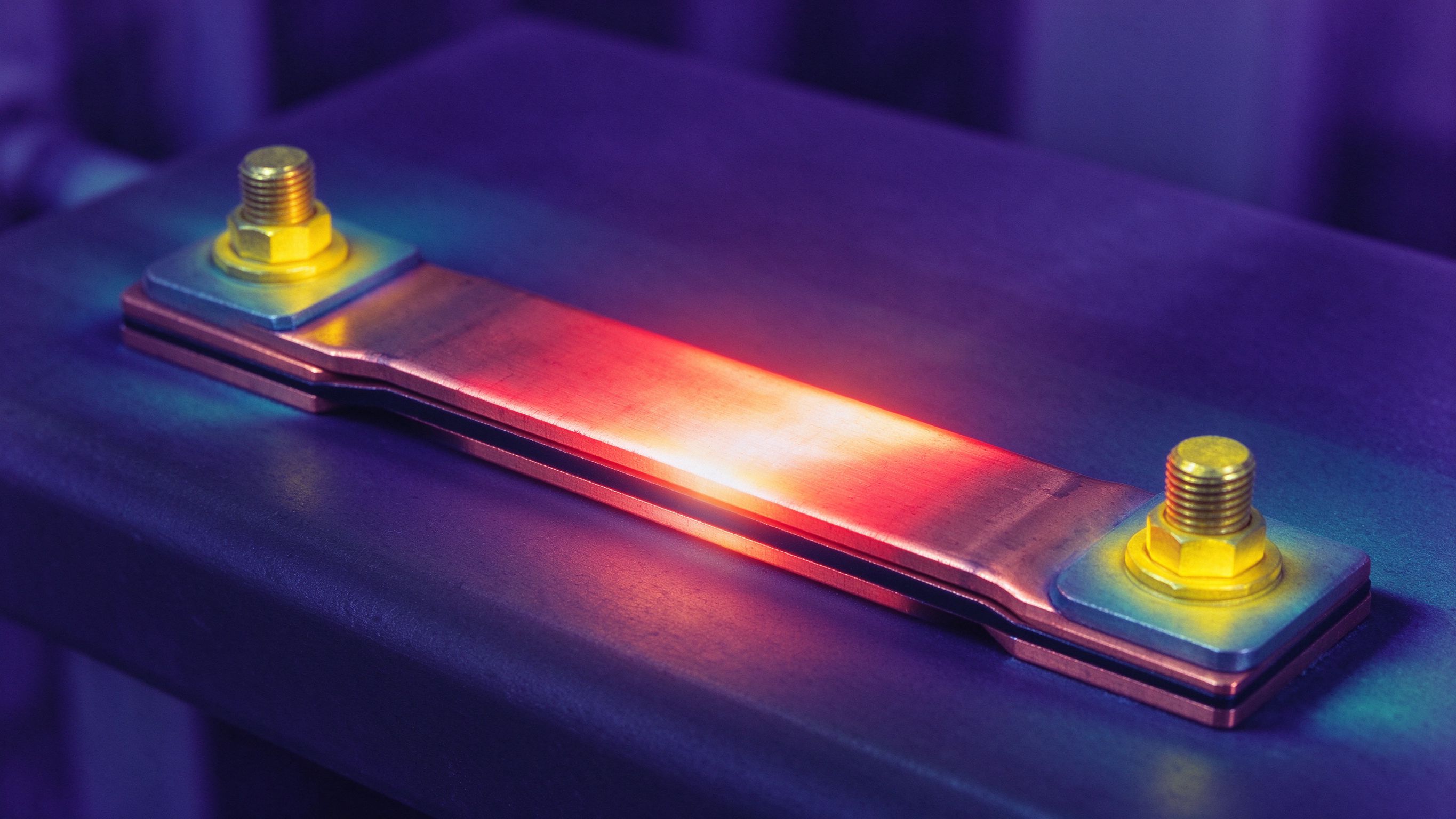
Heat is the second hidden cost of adding layers. Each dielectric layer is a thermal insulator — PET conducts heat far worse than copper — so a 6-layer stack conducts heat to its mounting surface less efficiently than a 2-layer assembly. At ~1000 A class currents, the temperature-rise budget of 30°C at rated current must be verified by measurement, not extrapolated from a single-plane calculation.
Practical mitigation: thicker edge copper, aluminium or copper heat-spreader plates on the outer planes, and bolted heat paths at mounting studs. If your application is a thermal-management-critical design — BESS rack bus, EV inverter DC-link, charging module — ask the fabricator for a measured temperature-rise curve at your exact current profile, including the ripple component.
| Attribute | 1-layer bar | 2-layer laminated | 4-layer laminated | 6-layer laminated |
|---|---|---|---|---|
| Typical use | Switchgear, ground bars | DC-link pairs, phase/neutral | 3-phase, dual DC pairs, EMI control | Complex converter/ESS zones |
| Stray inductance (1 m) | High (50-150 nH) | Low (5-20 nH) | Lower, field-cancelling | Lowest per path |
| Voltage class | Any, clearance-driven | Up to ~1.5 kV common | Up to ~3.3 kV with care | Up to 4.5 kV, PD-tested per layer |
| Thermal path | Direct | Good | Moderate | Needs spreaders/edge copper |
| Manufacturing complexity | Low | Medium | High | High + test burden |
| Relative cost | Base | 1.3-1.6x | 1.8-2.4x | 2.5-3.5x |
| Failure modes to manage | Creepage, joint fatigue | Edge PD, delamination | Edge PD, delamination, layer registration | PD per layer, thermal stack |
Cost ratios are typical ranges for C11000 copper, tin-plated assemblies and are intended as planning numbers, not quotes.
If the application is a renewable or storage inverter package, start from the 2-layer default and add layers only when a measured problem — inductance, EMI, or space — justifies them.
Four rules keep a multi-layer assembly from becoming a reliability problem:
For the mechanical mounting side of the same assembly, the vibration and bolted-joint design note is the companion read.
When the layer count is settled, the RFQ should carry enough data for a fabricator to quote without guesswork:
SHANYUAN engineers use exactly this checklist when quoting custom laminated busbar from 1 to 6+ layers on C11000 copper; the same inputs drive the test reports shipped with every assembly.
Start at the lowest layer count that meets the electrical spec, add layers only where inductance, EMI or space forces them, and verify with measurements — loop inductance, PD, temperature rise — not with the drawing. The three market articles published alongside this guide — Europe's grid spending, Southeast Asia's data center build-out and North American reshoring — all describe applications where this discipline is currently being tested in the field.
If you are unsure which configuration fits, send the circuit description and envelope and we will recommend the layer count with the test data to back it.
Layer count is the biggest single cost driver in a laminated busbar, so the cost model belongs in the selection framework. Copper dominates the material bill — at C11000 quality and 600-2500 A class currents, the conductor cross-section is set by temperature rise, and a thicker stack does not reduce the copper. What layers add is process cost: more film lamination passes, more registration tooling, more test time, and a higher probability of rework when an edge defect is found.
The comparison matrix in this guide puts a 4-layer assembly at roughly 1.8-2.4x a single bar and a 6-layer stack at 2.5-3.5x. Those multiples are planning numbers, but the shape of the curve is stable: each additional layer buys less incremental performance while costing a similar increment of money. The economic optimum is almost always the lowest layer count that passes the measured inductance and EMI spec — the current-sharing design article shows what happens when parallel planes are added for the wrong reason.
One cost lever buyers miss: the test package. A PD test per layer, a full temperature-rise run and a hipot at system voltage add real hours. Decide the test scope in the RFQ, not after the first quote, and the fabricator can price it transparently — which is what the supplier evaluation guide means by a complete scope of supply.
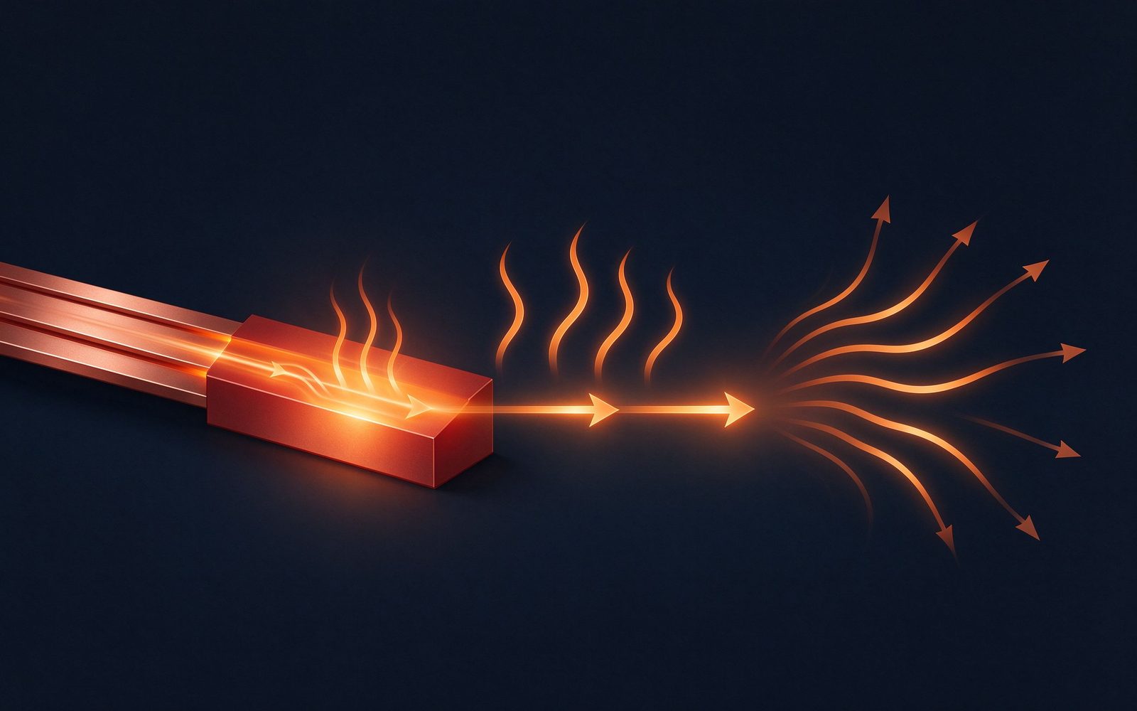
A busbar's rating is not a lookup — it is a calculation. Temperature rise is the real limi
Read article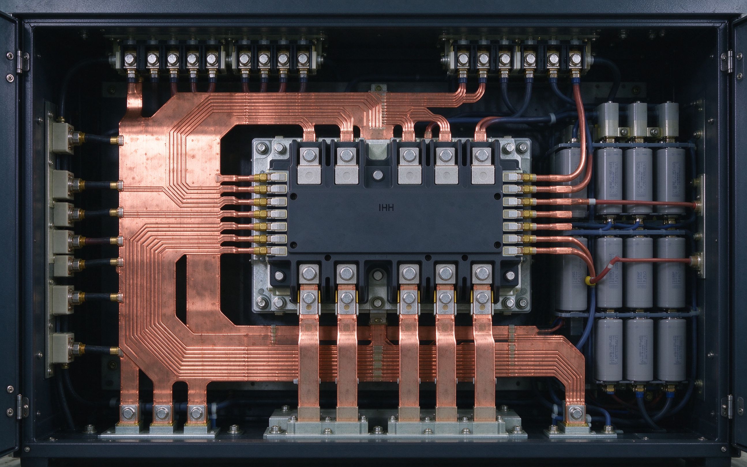
Higher switching speeds from SiC MOSFETs and modern IGBTs are pushing the DC-link busbar t
Read article
Daniel Richter is the chief electrical engineer at SHANYUAN Laminated Busbars, with 15 years in laminated busbar design and current-carrying systems. He leads electrical dimensioning, DC-link layout and thermal simulation for power converters, EV platforms and HVDC stations, and holds an M.Sc. in El
Send the current profile, voltage class and terminal types — our engineers reply within one business day.