When two busbars are paralleled, the intent is equal sharing — half the current, half the loss, twice the rating. The reality is governed by skin effect and proximity effect: AC current concentrates where the field allows it, and the distribution depends on geometry, frequency and layer spacing. In a laminated busbar, the layer-to-layer proximity effect is so strong that effective AC resistance can reach 2–5× the DC value (NovaSolver, 2026), and designers who ignore it size the copper by DC math and measure an overheated part. This guide puts the numbers on current sharing — and shows why thin layers beat thick plates.
When two busbars are paralleled, the intent is equal sharing — half the current, half the loss, twice the rating. The reality is governed by skin effect and proximity effect: AC current concentrates where the field allows it, and the distribution depends on geometry, frequency and layer spacing. In a laminated busbar, the layer-to-layer proximity effect is so strong that effective AC resistance can reach 2–5× the DC value (NovaSolver, 2026), and designers who ignore it size the copper by DC math and measure an overheated part. This guide puts the numbers on current sharing — and shows why thin layers beat thick plates.
Paralleling busbars is the classic way to scale current capacity: two bars per phase, four bolts per phase, 'double the rating'. The assumption is uniform division of current. The physics is more complicated — the division is set by the AC impedance of each path, and AC impedance depends on skin effect, proximity effect and the magnetic interaction between the paths.
Current sharing depends on connection quality too — see bus bar connections and connectors for joint design, and low-inductance design for loop control.
At DC, paralleling works exactly as expected: current splits by resistance, and equal bars share equally. At 50/60 Hz, and especially at switching frequencies with harmonics, the sharing degrades — in extreme cases one path carries most of the current while the parallel path barely contributes, defeating the purpose of paralleling entirely.
AC current concentrates toward the conductor surface, decaying exponentially with depth. The relevant metric is skin depth δ, and the design rule is the ratio t/δ (conductor thickness to skin depth): when t/δ > 3, almost no current flows in the central part of the conductor (NovaSolver, 2026). At 50/60 Hz the skin depth in copper is about 9.4 mm, so conductors thinner than ~10 mm are barely affected — but harmonics and switching frequencies shrink δ dramatically, and the effective resistance rises (A&J Link, 2026).
The counterintuitive consequence: at high frequency, a 10 mm-thick bar carries almost no more current than a 3 mm bar of the same width — thickness beyond a few skin depths is wasted copper.
Proximity effect is skin effect's neighbor: the magnetic field from an adjacent conductor distorts the current distribution inside its partner. In a three-phase busbar run, each bar's current is pushed to the far faces by the neighboring phases; in a laminated P/N pair, the opposing conductor's field concentrates current on the facing surfaces.
The laminated case is the strongest form of proximity effect, because the P and N layers are separated by thin dielectric — centimeters or even millimeters apart. The result, per NovaSolver's 2026 analysis, is that laminated busbar effective AC resistance can reach 2–5× the DC value. This is not a defect; it is the operating condition of the geometry, and it must be included in the loss calculation.
Copper skin depth: ~9.4 mm at 50 Hz, ~6.6 mm at 100 Hz, ~2 mm at 1 kHz, ~0.7 mm at 10 kHz, ~0.2 mm at 100 kHz. For a 50/60 Hz distribution busbar, a 10 mm bar uses its full thickness; for a switching-frequency current component at 10–20 kHz, only the outer ~1 mm carries significant current — so the effective resistance at harmonic frequencies is much higher than the DC value.
This is why harmonic content matters in the rating: a converter-fed busbar carrying fundamental plus switching-frequency harmonics must be rated on the harmonic-weighted loss, not the 50 Hz value. The practice is documented in the ampacity calculation guide we published this week.
Adding a parallel bar reduces each bar's share — but not linearly. The proximity field of the new bar raises the AC impedance of the first, and the benefit of each added bar diminishes. Published Japanese busbar engineering notes (Dou-Busbar, 2026) describe exactly this 'head limit': after a certain number of parallel bars, adding another delivers almost nothing, because the current crowds into the outer faces of the outer bars and the inner bars carry little.
The practical engineering answer is spacing and geometry: parallel bars separated by more than their width interact less (TRAFOLO, 2026, advises treating results as optimistic when phase spacing is under about twice the bar width), and edge-mounted or vertically-stacked arrangements change the sharing entirely.
It is not just the conductors that see proximity effects. Eddy currents induced in nearby steel — enclosure panels, mounting plates, structural steel — add loss and heat. A busbar run mounted on an unpainted steel frame can lose measurable capacity to induced eddy currents in the frame, at the switching-frequency harmonics most of all.
The mitigation is non-magnetic mounting: non-ferrous brackets, aluminum or stainless hardware, and clearance from steel enclosures. The bracket designs we use for power electronics busbars are specified for exactly this reason.
The solution to skin and proximity loss is not thicker copper — it is more, thinner layers. A laminated busbar with 6 layers of 1 mm copper has the same copper volume as one 6 mm bar, but each layer operates within its skin-depth budget and the P/N pairing cancels field between adjacent layers. The effective AC resistance at switching frequencies is dramatically lower, which is why multi-layer laminates outperform thick single bars in converter duty (A&J Link, 2026).
This is the core argument for laminates in SiC and high-frequency IGBT stages: not just low loop inductance (covered in our DC-link design article) but lower AC loss per amp at the frequencies that matter.
The same physics appears in branched distribution: when current splits between a short path and a long path, the AC impedance difference — not just resistance — decides the split. A&J Link's 2026 analysis of branch sharing shows the mechanism precisely: when conductor thickness t >> δ, increasing thickness barely changes the effective conductive area, so the AC impedance difference between branches stays small; but when t approaches δ, the eddy loss of the longer path rises sharply and its AC impedance climbs — most current flows to the short path, a severe imbalance.
The design rule: keep branched paths symmetric in geometry and length, or compute the AC impedance split explicitly rather than assuming resistance-only sharing.
Layer design follows the frequency content. For a 50 Hz distribution laminate, 2–3 mm layers are comfortable within skin-depth budgets. For a switching-frequency DC-link carrying 10–20 kHz ripple, 0.5–1 mm layers begin to make sense, with the layer count rising to keep the cross-section. The penalty for over-thick layers is not just lost copper — it is eddy loss inside the conductor itself, which shows up as unexpected heating and an ampacity shortfall.
The thermal management guide connects the layer stack to the temperature budget, closing the loop between the electrical and thermal calculations.
Calculated sharing is a prediction; measured sharing is the truth. Verification methods: current probes on each parallel path at full current, Rogowski coils around individual laminates, or thermal imaging — the bar that carries more current runs hotter, and the thermogram reveals imbalance directly. AC resistance measurement by impedance analysis across the frequency range captures the skin/proximity contribution numerically.
For production, we combine design verification with lot-level DC resistance checks and first-article AC impedance measurements on converter-grade parts, per the quality system.
Five rules control sharing in practice: (1) keep parallel paths geometrically symmetric — equal length, equal cross-section, mirror-image routing; (2) space parallel bars beyond proximity range where envelope allows (phase spacing ≥ 2× bar width); (3) prefer thin multi-layer construction over thick single bars when harmonic content is significant; (4) avoid steel in the return path and near-field; and (5) verify by measurement at the worst operating frequency, not just DC resistance.
These rules apply to distribution busbars and laminates alike, and they are the first five items in our design review for every custom busbar.
Converter-fed busbars carry fundamental plus switching-frequency harmonics, and the harmonic content decides the real loss. A 50 Hz-rated bar feeding a PWM converter may run well within its catalog rating at DC but overheat at the harmonic-weighted loss. The correct method is a Fourier decomposition of the current waveform, a loss calculation at each significant harmonic using the frequency-dependent AC resistance, and summation into a total loss versus the thermal budget — the approach in our ampacity guide.
The multi-layer laminate is the standard fix, converting a loss problem into a layer-count decision.
The proximity effect is usually described as a loss. In a laminated P/N pair it has a redeeming feature: the face-to-face current paths partially cancel each other's fields, which is precisely what makes the low-inductance DC-link possible. The field cancellation also reduces the external field the laminate radiates to neighboring steel and cables — an EMI and eddy-loss benefit that bare bars do not have.
So the same geometry that costs 2–5× AC resistance in the internal loss calculation buys the low inductance and low external field that converter design needs. The manufacturing process article describes how the layer stack is built and aligned.
The failure modes of ignoring sharing physics are concrete: an over-specified parallel bar that still overheats; a branch that carries 80% while its twin carries 20%, failing the temperature-rise test at half the intended load; a converter-fed bar that passes bench tests at DC and fails in service at switching frequency; eddy-current losses in the enclosure that raise the cabinet temperature and derate the whole assembly.
Each is a design-time fix, and each shows up in the verification stage if the sharing calculation was done honestly.
Current sharing is the physics that makes laminated busbars the right answer for high-frequency power: skin effect and proximity effect penalize thick single conductors, and the multi-layer, face-to-face laminate is the geometry that shares current, cancels field and controls AC loss at once. The numbers — 9.4 mm skin depth at 50 Hz, t/δ > 3 wasted copper, 2–5× AC resistance in laminates, diminishing returns beyond a few parallel bars — are the vocabulary of the design discussion.
When you size the next DC-link or distribution busbar, run the sharing calculation before the thermal one. Our engineers do both on every inquiry, and the result is a part that carries what the nameplate says, at the frequencies the system actually runs.
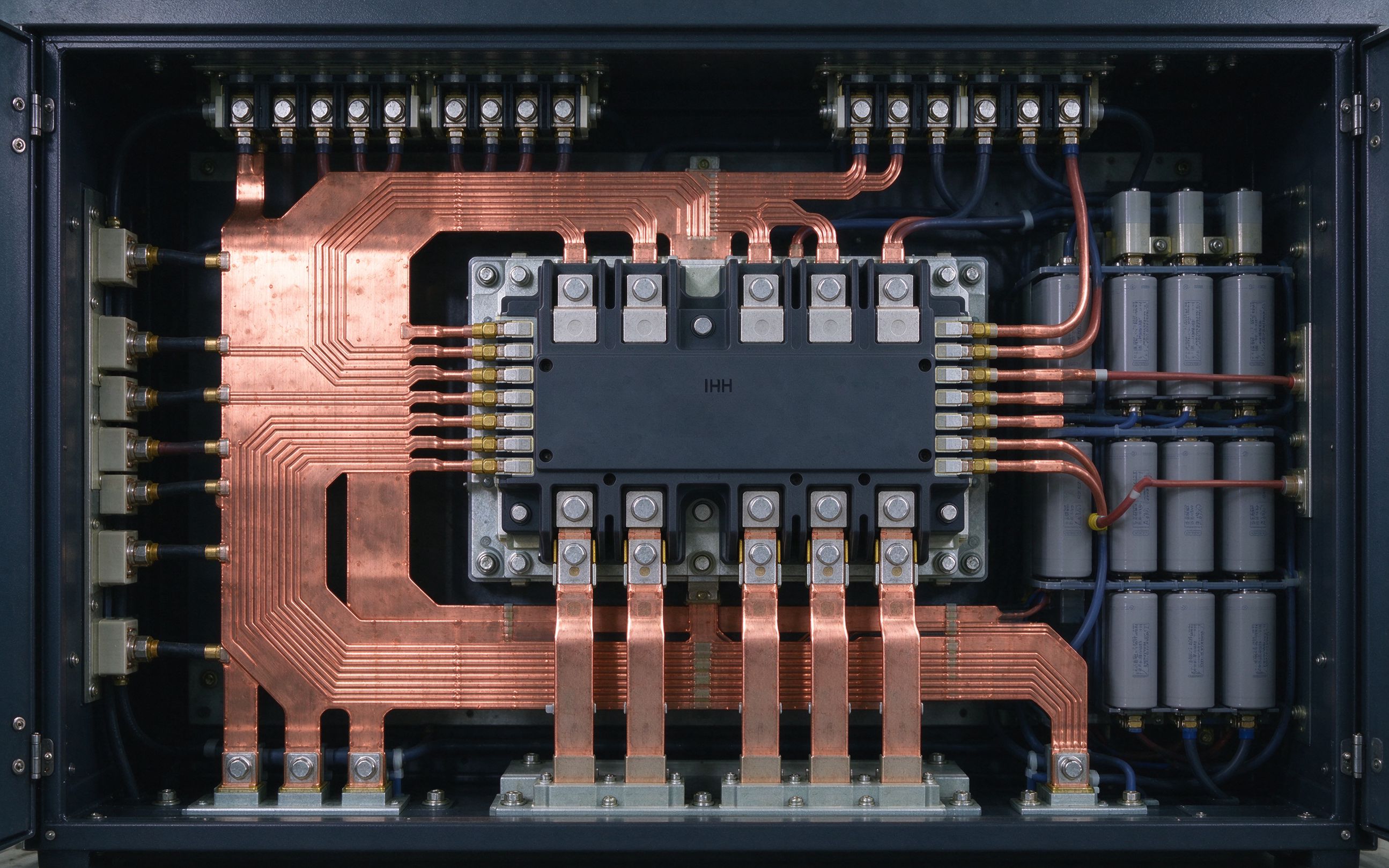
The inverter that dominated 2026's solar tenders is no longer a small box: 300 kW-plus str
Read article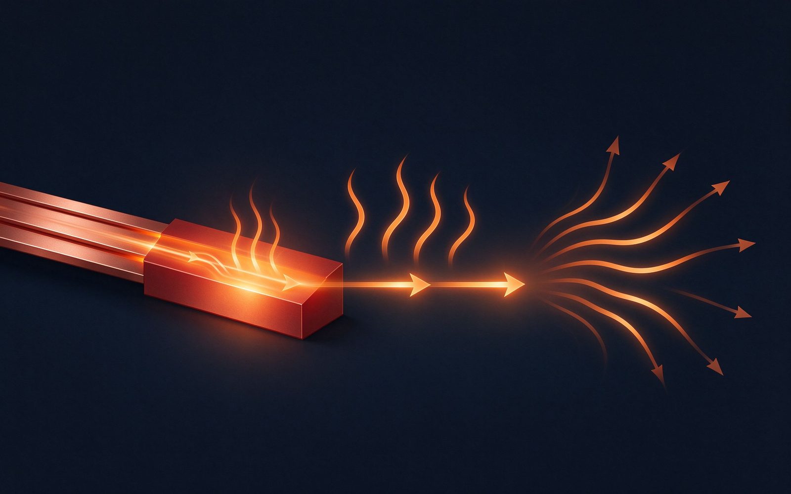
A busbar's rating is not a lookup — it is a calculation. Temperature rise is the real limi
Read article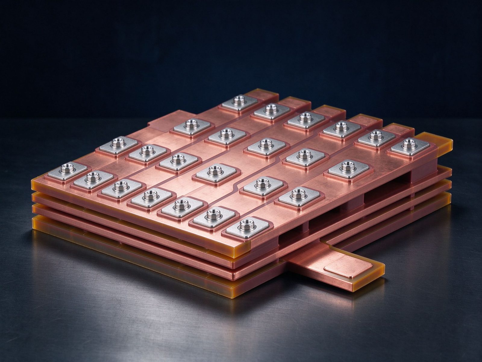
SiC is scaling up — literally. Eight-inch wafer capacity is expanding at double-digit CAGR
Read articleSend the current profile, voltage class and terminal types — our engineers reply within one business day.