Power semiconductors have been the headline story of the last decade in power electronics. SiC MOSFETs now switch five to ten times faster than legacy silicon IGBTs, and modern IGBT modules keep pushing edge rates higher. But every nanosecond of faster switching demands a commensurate reduction in stray inductance around the DC link. By 2026, the IGBT DC-link busbar and its SiC equivalent have moved from a mechanical afterthought to one of the most carefully simulated parts in the inverter stack. This article from the SHANYUAN engineering team explains why, and what designers should change in their 2026 programs.
Power semiconductors have been the headline story of the last decade in power electronics. SiC MOSFETs now switch five to ten times faster than legacy silicon IGBTs, and modern IGBT modules keep pushing edge rates higher. But every nanosecond of faster switching demands a commensurate reduction in stray inductance around the DC link. By 2026, the IGBT DC-link busbar and its SiC equivalent have moved from a mechanical afterthought to one of the most carefully simulated parts in the inverter stack. This article from the SHANYUAN engineering team explains why, and what designers should change in their 2026 programs.
When a transistor turns off, the current in the stray loop inductance does not stop instantly. The inductor fights the change, generating a voltage spike V = L · di/dt. With a modern SiC module switching at 5-10 kA/µs, even 20 nH of loop inductance produces a 100-200 V spike on top of the DC-link voltage. At an 800 V DC bus, that spike can push the device toward its breakdown limit.
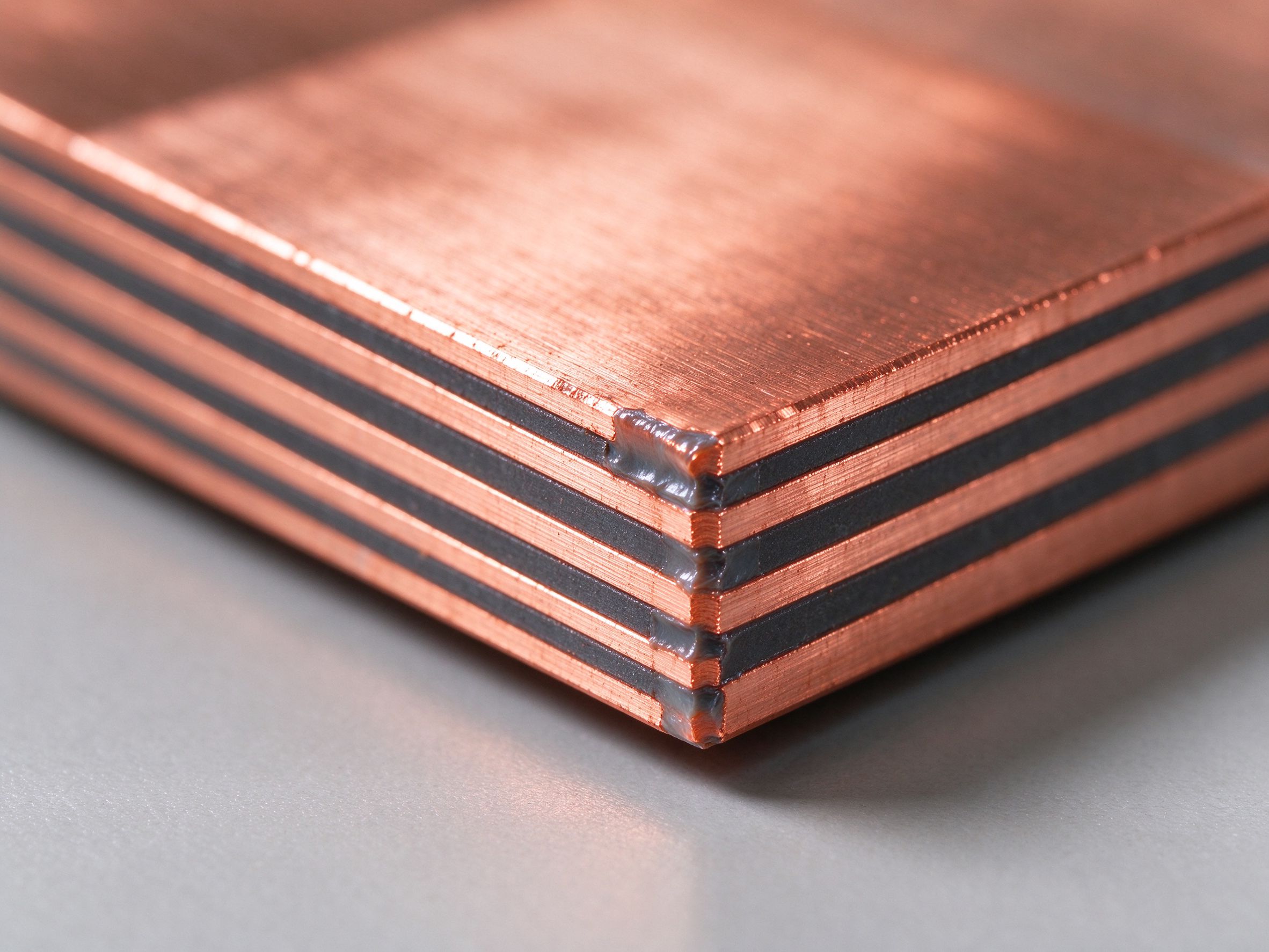
The math is unforgiving. A lower switching-loop inductance is the only way to run faster edges safely, and the dominant contributor to that loop inductance is the physical path between the DC-link capacitors and the power modules. That path is exactly what a laminated busbar controls. A well-designed low-inductance busbar interleaves the positive and negative rails so that currents flow in opposite directions in adjacent copper layers, canceling magnetic field and driving loop inductance down to the 10-15 nH range.
The market trajectory reinforces the point. TrendForce and McKinsey both track SiC adoption across EV traction inverters, photovoltaic string inverters, and industrial drives. As SiC content per inverter rises, the inductance budget tightens. A 2018-era IGBT inverter tolerated 40-60 nH of DC-link inductance; a 2026 SiC inverter expects 15 nH or less. That is the same order of improvement that the busbar has to deliver, and it cannot be fixed with a snubber capacitor alone. Snubbers help, but they add loss, weight, and board space; the cheapest way to hit the inductance target is to design the busbar right the first time.
The consequence of getting it wrong is not theoretical. A DC link that loops at 40 nH in a SiC inverter will either force the designer to derate the bus voltage, add bulky snubber capacitors, or accept higher device failure rates. None of those is attractive. The better path is to treat the busbar as part of the power-loop design, not as a mechanical bracket that happens to carry current. That means involving the busbar supplier at the schematic stage, not after the PCB and capacitor layout are frozen.
For the vehicle-side context, see our overview of 800V EV busbar trends. For the manufacturing process behind the part, read laminated busbar manufacturing process.
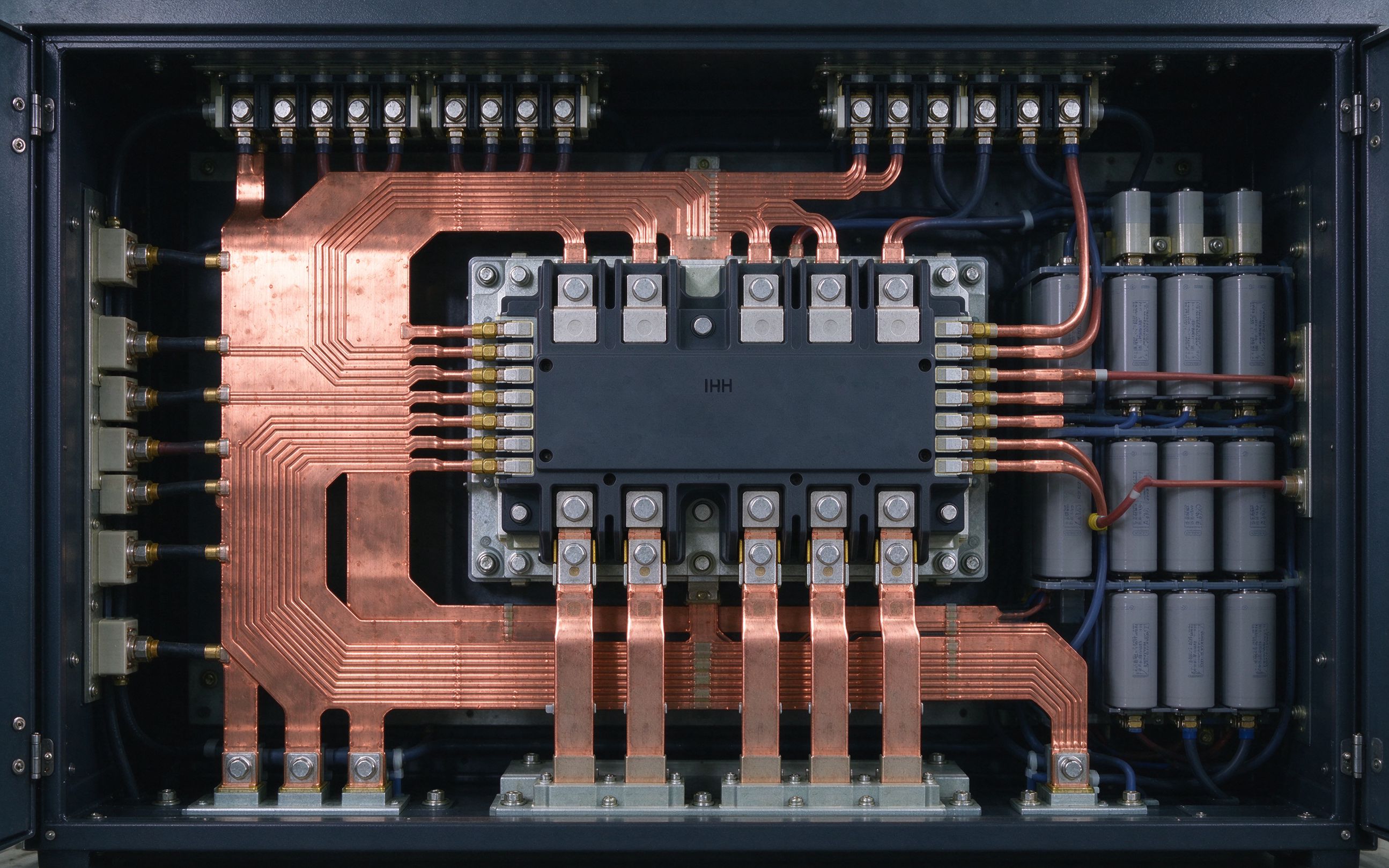
A DC-link busbar is not a flat sheet of copper. It is a precision geometry that has to mate simultaneously with the capacitor bank on one side and the power module on the other. Two design rules dominate.
First, minimize the loop area between the DC+ and DC- terminals of each capacitor and the AC terminals of the module. The shorter and flatter the loop, the lower the inductance. Second, interleave layers so that current in adjacent copper sheets flows in opposite directions. The mutual inductance cancellation is what drives total inductance down, not just the raw cross-section.
| Design Feature | Inductance Impact | Typical Target |
|---|---|---|
| Single-layer busbar, no interleaving | High, 40-80 nH | Avoid for SiC |
| Two-layer laminated, DC+ / DC- interleaved | Moderate, 20-30 nH | Legacy IGBT OK |
| Multi-layer, symmetric capacitor-to-module | Low, 10-15 nH | SiC target |
| Symmetric current sharing across parallel modules | Prevents uneven stress | <5% imbalance |
Symmetry matters more than most designers expect. If the DC-link capacitors are clustered on one side of the busbar, the module closest to the capacitors sees a lower-inductance loop than the one farthest away. The result: one module switches hard and the other switches soft, with uneven thermal and electrical stress across the paralleled modules. A symmetric layout, with capacitors distributed evenly around the module terminals, costs a little more footprint but pays back in even stress and longer life.
SHANYU runs a DFM review on every inverter busbar, looking at the capacitor footprint, the module footprint, and the thermal envelope before we quote. We use C11000 copper, tin-plated where it touches other hardware, and PET or Nomex dielectric depending on temperature class. Aluminum is available on select lower-current layers when weight is critical.
A low-inductance busbar that cracks under thermal cycling is useless. Inverters heat up and cool down with every drive cycle; the copper, the dielectric, and the bolted terminals all expand at different rates. Two mechanical failures are common.
The first is fatigue at the terminal hole, where copper flexes against a bolted bushing. The fix is reinforcement: a thicker local tab, a stress-relief slot, or a softer plating that yields before the copper does. The second is delamination at the lamination edges, where repeated heating lifts the dielectric away from the copper. Full edge sealing and controlled lamination pressure prevent this. Every SHANYU busbar is edge-sealed and 100% tested with hipot, insulation resistance, and continuity before shipment.
Engineering note: the busbar and the capacitor supplier should be on the same page early. Capacitor terminal stiffness and position set the mechanical interface; changing either late in the program re-opens the inductance model.
Vibration is the other boundary condition. An inverter mounted in a truck, a locomotive, or a wind turbine sees continuous random vibration. A bolted busbar that is fine on a bench can loosen in the field unless the torque sequence, lock-washer choice, and terminal stiffness are designed together. Our busbar design guide and the companion terminal connection guide walk through the joint checklist. For traction inverters, which see both vibration and thermal cycling, we recommend torque-to-yield bolts on the main DC terminals, with a documented re-torque interval for service. For industrial and solar inverters, which see less vibration but more continuous duty, a controlled-torque bolt with a lock washer is usually sufficient. The choice is set by the application, and we will call it out in the DFM note.
Partial discharge is the other silent failure mode, especially at 800 V and above. Air voids between the copper and the dielectric, or along the cut edges, can glow with partial discharge when the inverter switches. Over months, that erosion eats through the insulation. Full edge sealing and controlled lamination pressure are the two process steps that prevent it. Every SHANYU busbar is edge-sealed, and we can run partial-discharge testing on sample lots when the application requires it.
Cost is the last thing designers ask about, but it matters. A low-inductance SiC busbar uses more precision copper and tighter layer registration than a legacy IGBT part. The good news is that the marginal cost is small relative to the system cost: a SiC inverter costs thousands of dollars in modules and capacitors, and the busbar is a small fraction of that. Skimping on the busbar to save a few dollars per unit is a bad trade when it compromises the switching performance that justifies the SiC choice in the first place. Design the loop right, qualify it, and then lock the geometry for the program. The payback is simpler thermal design, smaller snubbers, and more headroom on the device rating — all from a part that costs a fraction of the inverter itself. If your 2026 program is pushing switching speeds higher and the DC link is the sticking point, bring us the module and capacitor outlines early. We will run the inductance estimate, flag the geometry risks, and give you a fixed-price budget within one working day. Samples follow in 5-7 working days, and mass production in 2-3 weeks once drawings are frozen. Every unit ships with 100% hipot, insulation-resistance, and continuity test records so your incoming inspection is a paperwork check, not a re-validation. We also support customer witness testing at our Rizhao facility for programs that require third-party verification before mass production begins. We ship internationally by sea and air from our Rizhao, Shandong facility, supporting programs worldwide with reliable lead times.
SiC MOSFETs and modern IGBTs both benefit from a low-inductance DC link, but the design emphasis shifts. SiC switches faster, so the absolute inductance target is tighter (often under 15 nH) and dv/dt control matters more for EMI. IGBTs switch slower, so the inductance budget is looser, but the current levels are often higher, so thermal performance and contact area dominate.
Practical differences in 2026 designs include:
Whatever the device, the procurement discipline is the same: lock the semiconductor and capacitor early, because the busbar geometry is downstream of those choices. SHANYU's DFM-first process means we can turn a custom busbar quote around in one working day once those three pieces (device, capacitor, envelope) are on the table.
An IGBT DC-link busbar is not a commodity. It is a precision component that has to survive 15 years of vibration and thermal cycling inside an inverter enclosure. When you evaluate a power electronics busbar supplier, look for evidence of in-house process control rather than assembly of bought-out subcomponents.
SHANYU has run our own lamination, stamping, laser cutting, and test lines in Rizhao, Shandong since 2012. We do not outsource the lamination step, because that is where the inductance and insulation quality are actually set. Production output is 100% electrically tested, and samples are available in 5-7 working days with mass production in 2-3 weeks. We ship internationally by sea and air.
Quality expectations for a DC-link busbar should include: 100% hipot and insulation-resistance test on every unit, documented layer registration tolerance, material certificates for the copper and dielectric, and a sample-approval process before mass production starts. We also support customer witness testing at our Rizhao facility for programs that require it. If you are specifying a SiC or IGBT inverter for a 2026 program and want to buy laminated busbars from a busbar OEM that understands the switching loop, send us the module and capacitor outline drawings. We will come back with a geometry recommendation, a stray-inductance estimate, and a fixed-price budget within one working day through /contact/ or busbar@shanyo.com.
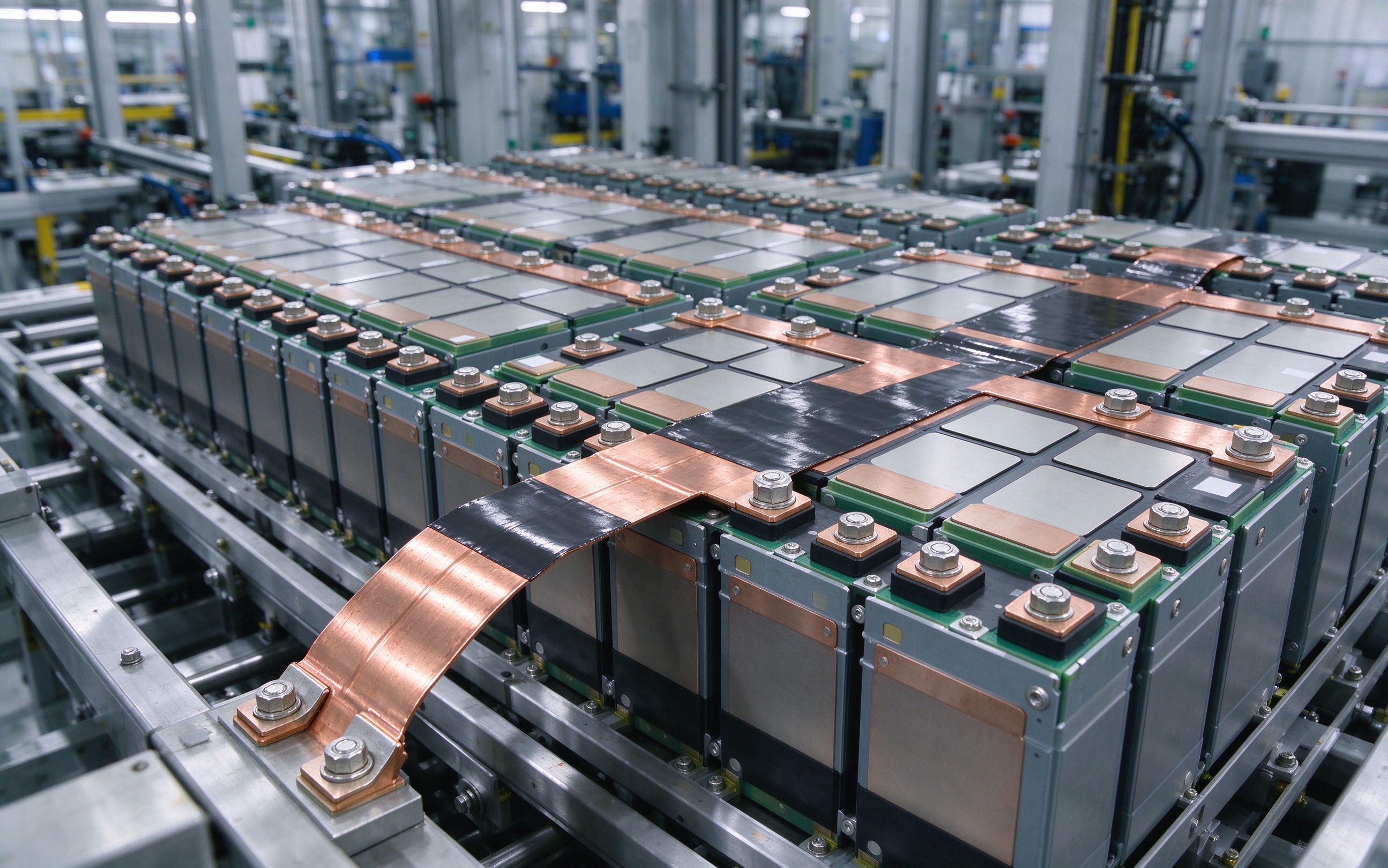
The shift from 400V to 800V vehicle architectures is rewriting the electrical layout insid
Read article
Copper busbar current rating is not a single number. It is a starting ampacity adjusted by
Read articlePET, Nomex and DLF epoxy are the three dielectrics we laminate into SHANYUAN busbars every
Read articleSend the current profile, voltage class and terminal types — our engineers reply within one business day.
Send drawings, current ratings and voltage class — DFM feedback and a quotation within one business day.