EMC failures at the test bench are rarely a component problem and almost always a loop problem. The switching transient in a power stage drives current through a loop defined by the DC-link busbar, the module terminals and the decoupling capacitors — and every square millimeter of that loop is an antenna. Laminated busbar design is the first and most effective EMI control in the converter, and it works before any shield or filter is added. This guide explains the mechanism and the layout rules that make a converter quiet by design.
EMC failures at the test bench are rarely a component problem and almost always a loop problem. The switching transient in a power stage drives current through a loop defined by the DC-link busbar, the module terminals and the decoupling capacitors — and every square millimeter of that loop is an antenna. Laminated busbar design is the first and most effective EMI control in the converter, and it works before any shield or filter is added. This guide explains the mechanism and the layout rules that make a converter quiet by design.
Every switching action produces two EMI signatures. The differential-mode signature comes from the loop current changing fast — di/dt through the DC-link loop that includes the busbar, the module and the capacitors. The common-mode signature comes from the voltage changing fast — dv/dt across parasitic capacitance between the switching node and ground, through heatsinks, enclosures and cables. Both scale with switching speed, and both are controlled by geometry before they are controlled by filters.
The uncomfortable consequence: the EMI fix is mostly decided at the layout stage, and the layout stage is where the busbar geometry gets locked. A converter that fails EMC at 100 kHz to 1 MHz usually needs a layout change, not a bigger filter.
The differential-mode EMI current follows the path of least inductance, and that path is the DC-link loop: positive busbar to module to negative busbar to capacitor and back. Stray inductance in that loop stores energy that becomes voltage overshoot at turn-off — the ringing that radiated emissions track. The loop's area and length set both the inductance and the antenna efficiency, which is why the same schematic can pass EMC in one layout and fail badly in another.
The design quantity that matters is loop inductance — measured in nanohenries, not the rating of the components. Our loop inductance measurement guide covers how it is measured and verified; the layout rules below are the design side of the same equation.
Fuji Electric's power-module application guidance states the principle directly: a laminated busbar places the positive and negative conductors in parallel layers separated by thin insulation, which reduces the loop area and provides strong magnetic-field cancellation. Currents flowing in opposite directions in the two layers generate opposing fields that cancel, shrinking the effective loop the switching transient sees. The same physics that lowers inductive voltage overshoot also lowers the differential-mode antenna efficiency.
This is the argument for multi-layer laminated busbars over a pair of separate bars or cables: the EMI control is built into the conductor geometry, before any shielding component is added. For the converter designer it is the cheapest nanohenry reduction available — and in a market where copper supply is tightening, it is also the most metal-efficient one.
The layout rules come from the field-cancellation principle, and they are specific enough to be a checklist. Keep the positive and negative layers close — the dielectric thickness directly adds to loop height. Maintain the overlap all the way to the module terminals — where the layers separate, the loop opens. Avoid narrow necks in the conductor path; they concentrate current and add inductance. Minimize terminal extensions beyond the module footprint. Use symmetrical paths to parallel modules so the currents share evenly. And position capacitor connections directly across the DC terminals, not at the far end of the busbar.
Each rule is a loop-area decision. Our current sharing design guide covers the parallel-module symmetry side; the FEM impedance simulation guide shows how to verify the loop numerically before hardware exists.
Common-mode current does not follow the schematic — it follows parasitic capacitance. The switching node (typically the IGBT/SiC module output) couples through the module baseplate to the heatsink, through the heatsink to the enclosure and ground, and through cables and mounting hardware back to the DC source. Every path is a small capacitance, and at dv/dt rates of tens of kilovolts per microsecond, small capacitances conduct real noise current.
Controlling common mode is about managing those parasitic paths deliberately. The EMI fix is a grounding and coupling plan: heatsink ground connection, cable routing, and an understanding of where the noise current returns. Fuji Electric's EMC guidance for IGBT modules treats common-mode reactors, arresters and input filters as a system placed where the coupling paths actually are.
The heatsink is the biggest parasitic capacitor in the converter, and its grounding decides what happens to the coupled noise. A properly bonded and grounded heatsink provides a low-impedance return that keeps common-mode current inside the converter; a floating or poorly bonded one turns the heatsink into an antenna. The guidance from power-module manufacturers is consistent: ensure proper bonding and grounding of the heatsink to prevent radiated fields, and use metal enclosures or shields around the module to contain emissions.
For a converter designer this is a mechanical-electrical decision made together: mounting hardware, conductive gaskets, bonding straps and enclosure continuity all belong in the EMC review, not the mechanical review. The same discipline governs power electronics busbar integration — the busbar, the module and the heatsink form one electrical system.
Metal enclosures and shields contain radiated emissions, but a shield is only as good as its connections. A metal cover with slots, gaps and an unpainted seam is a collection of slot antennas; the shield's effectiveness comes from electrical continuity — multiple bonded contact points, conductive gaskets at openings, and a clean low-impedance connection to the ground plane. The same rule applies to internal shield plates between power stage and control electronics.
Shielding is the last line of defense, not the first. It is most effective when the loop and common-mode controls are already working, because then the shield contains residual low-level noise instead of absorbing a broadband failure. Designers who skip the layout work and add a shield usually discover the shield needs to be huge to compensate.
Snubber networks control the turn-off voltage transient that ring carries into the radiated spectrum. An RC snubber across the module clamps the overshoot and damps the ringing, but its effectiveness is entirely placement-dependent: the snubber must sit as close to the module terminals as physically possible, inside the switching loop, or its own lead inductance adds back the loop it is supposed to tame. This is why snubber capacitors and resistors are integrated into DC-link busbar assemblies in high-speed designs — the busbar carries the snubber network at the terminal position.
For SiC converters switching at 100 kHz and beyond, snubber placement stops being a refinement and becomes the difference between a passing and a failing radiated test. Designers should ask the busbar supplier for integrated snubber capability, not add a loose component after the layout is frozen.
Filters are the systemic control, and their placement follows the coupling paths. A common-mode choke on the input line is effective for controlling noise up to the several-MHz band, which matches the first harmonics of typical IGBT switching. Differential-mode filtering needs the loop current to pass through the filter elements, which means the filter and the loop must be in the same circuit path. The layout rule: filters belong at the converter boundary, between the noisy power stage and the clean outside world.
Filter size is a function of how much noise the layout lets out, which is why the same compliance budget is met with a small filter on a well-laid-out converter and a large one on a poor layout. The harmonic current rating guide covers the differential-mode side of the sizing story.
EMC measurement is a controlled experiment: a line impedance stabilization network presents a defined impedance (typically 50 ohms) to each line, converting conducted noise current into a measurable voltage against the limit line. The measured level is only meaningful if the setup is right — cable routing, ground plane, and the LISN configuration are part of the measurement, not part of the converter. Comparing levels across setups is how EMI debugging goes in circles.
The practical discipline is to measure the same configuration every time: same LISN, same cable lengths, same ground reference. For the busbar design loop, the key measurement is the double-pulse test — the turn-off transient on the switching loop is the radiated spectrum in embryo, and our measurement guide explains how to extract and interpret it.
Silicon carbide switches faster, which is the point — and the problem. Faster dv/dt and di/dt spread the EMI spectrum to higher frequencies where shielding and filtering cost more. The 10 kV SiC designs now emerging push the same challenge to another octave. The response is the same geometry discipline, applied harder: minimum loop inductance, capacitor placement at the module terminals, integrated snubbers, and common-mode paths managed from the start.
Our SiC/IGBT DC-link busbar analysis covers the current generation; the SiC module market piece tracks how fast the industry is moving. The engineering message is stable: the faster the switch, the more the busbar layout is the EMC design.
Decoupling capacitors are the loop's terminus: the switching transient current circulates from the module through the busbar to the capacitors and back. Place the capacitors across the DC terminals, inside the loop, and the circulating current stays local and small; place them at the far end of the busbar and every millimeter of busbar between module and capacitor joins the loop. The same logic applies to snubber capacitors — proximity to the module is the design variable.
This is why DC-link capacitor assemblies and laminated busbars are engineered as one part in modern designs — the inverter DC-link busbar integrates the capacitor footprint into the conductor geometry. The EMI consequence of the integration is measurable and repeatable: shorter loop, lower inductance, less differential-mode emission.
The EMC design review for a power stage is a short checklist. Is the DC-link loop area minimized — layers close, overlap to terminals, no necks? Are capacitors across the terminals, not at the busbar end? Is the heatsink bonded with a low-impedance ground connection? Is the switching node kept short and away from sensitive circuitry? Are snubbers inside the loop at the module terminals? Are shields continuous, bonded and gasketed? Are filters at the boundary with the coupling paths understood? And is the measurement setup fixed so comparisons are valid?
A design that passes the checklist usually passes EMC on the first or second bench attempt. A design that fails the checklist usually fails EMC regardless of filter budget, and the fix is a layout revision — which is why low-inductance design resources should be read before the layout is committed, not after the test fails.
Every EMC consultant has met the project that adds shields, ferrites and filters to a converter whose real problem is a loop. The symptoms are diagnostic: the fix budget keeps growing while the margin does not, or the emission profile has a shape that matches a physical geometry rather than a harmonic set. When the radiated signature tracks the switching-loop geometry, the answer is a layout change, and no amount of bolt-on shielding substitutes.
The professional move is to measure the loop inductance, review the layout against the checklist above, and fix the geometry first. The FEM impedance simulation guide lets a team verify the loop on the drawing before cutting copper, which is both faster and cheaper than the shield-and-test loop.
The busbar is the EMI design, so the busbar supplier is an EMC engineering partner, not a fabrication vendor. The productive conversation starts with the switching parameters: frequency, di/dt, dv/dt, module package, capacitor plan. From those, the supplier derives the layer stack, the overlap, the terminal position, the snubber footprint and the measurement plan. A custom busbar program built this way converges on a quiet design in two or three layout iterations instead of an EMC campaign.
At SHANYUAN the engineering and test capability includes loop-inductance measurement and FEM verification, so the EMI conversation starts with numbers. Contact the engineering team with the switching parameters and let the layout work begin before the enclosure design locks the geometry.
EMC measurement splits into two domains with different physics. Conducted emissions travel on the cables and are measured through the LISN against limits defined from 150 kHz to 30 MHz; radiated emissions leave the enclosure and are measured with antennas against limits defined from 30 MHz up. The two spectra share a root cause — the switching transient — but their control paths differ: conducted needs the filter and layout, radiated needs the loop and the shield.
Reading a failed measurement correctly is half the fix. A conducted failure usually points at the input filter and the common-mode path; a radiated failure at the switching loop and the enclosure. The test report should say which domain failed at which frequency — that is the diagnosis the layout team needs.
The decoupling capacitors are the loop's energy reservoir, and their selection is an EMI decision as much as a power decision. The capacitor must deliver the switching current with minimal parasitic path — low ESL, low ESR, and a footprint that fits the busbar terminal position. Film capacitors dominate DC-link duty for their ripple capability and reliability; ceramic arrays serve snubber duty at the module terminals where the transient is fastest.
The selection rule is placement-led: the capacitor's terminals define the loop boundary, so the busbar layout should bring the capacitor pads across the module terminals rather than the reverse. The inverter DC-link busbar integrates that footprint as standard practice, and the current sharing design guide covers the parallel-capacitor symmetry that keeps the loop balanced.
The fleet context changes the EMI economics. A wind converter or a storage PCS that passes EMC once is a qualification event; a fleet that must pass repeatably, across manufacturing variance and field installation differences, is a design problem. The variance that breaks EMC repeatability is usually mechanical — capacitor placement drift, busbar tolerance, heatsink bonding quality — which is why the layout and assembly documentation matters as much as the test report.
Storage fleets have the extra constraint of density: containers pack converters, cables and cooling in tight envelopes, and the Indian storage build-out is shipping those containers by the thousands. Fleet EMC discipline — fixed layout rules, documented assembly tolerances, and a test campaign on first articles — is what keeps the pass rate high when volume ramps. The same fleet discipline extends to the long-duration plants now scaling, whose converter stages carry the identical EMI stakes.
Two failure investigations look different and share a root cause. A converter with a radiated emission signature that tracks the switching loop and a joint that runs hot under load are both telling the same story: the DC-link geometry is wrong. Loop inductance drives the voltage overshoot that radiates, and loop resistance and joint quality drive the temperature rise — and both are decided in the same busbar layout.
The diagnostic habit is to measure both before choosing the fix. A failure-mode analysis that covers thermal and electromagnetic modes together usually finds one root cause and one layout change that fixes both — cheaper than an EMI shield plus a maintenance campaign pursued separately.
A well-planned EMC campaign is iterative by design: pre-compliance measurements at the bench, a first full compliance test, a fix cycle, and a final verification. The pre-compliance stage is where the busbar layout gets validated — loop inductance measurement, double-pulse transient capture, and a conducted scan at the bench catch most problems before the chamber costs real money. The compliance test then confirms the design rather than discovering it.
After the campaign, the discipline continues into production: periodic re-verification on first articles and after any layout or component change, documented in the same format. The maintenance and measurement guide published today carries the trending discipline from the EMC lab into the field, because an EMC pass at qualification is a snapshot, and the fleet needs a trend.
Is shielding always needed for a power converter? No — most converters pass EMC with correct layout and grounding before any shield is added. Shielding contains residual emissions after the loop and common-mode paths are controlled; a shield that compensates for a poor layout is always bigger, hotter and more expensive than the layout fix. What is the single most effective EMI control? Loop-area minimization: laminated layers close together, overlap maintained to the module terminals, no narrow necks, capacitors across the terminals. That one discipline drives loop inductance, voltage overshoot and radiated emission together. How is busbar EMI verified? By measuring loop inductance and the turn-off transient with a double-pulse test, then confirming the full conducted and radiated spectra against CISPR limits in a compliance campaign.
Loop inductance decides how hard a SiC converter can switch. This guide covers the double-
Read article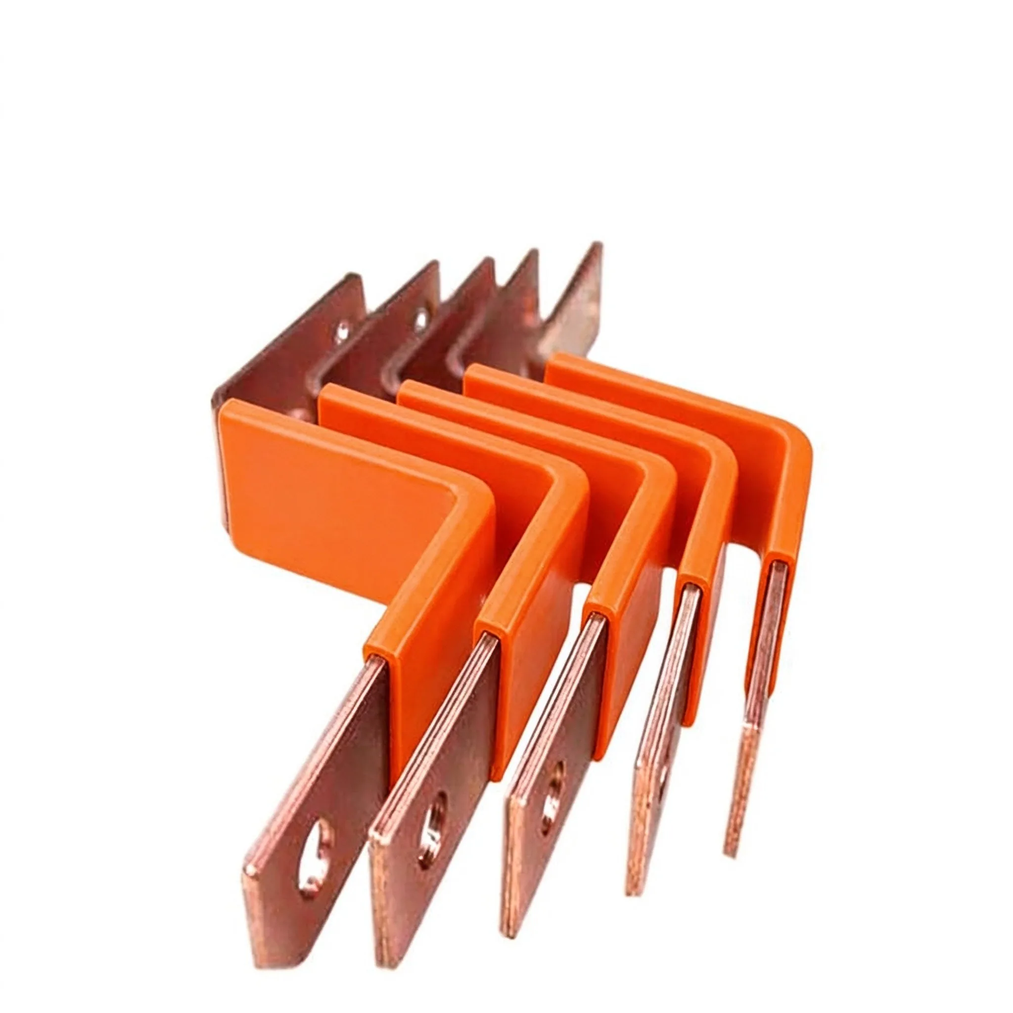
L_loop = Lp,P + Lp,N - 2Mp,PN: the partial-inductance equation behind every low-inductance
Read article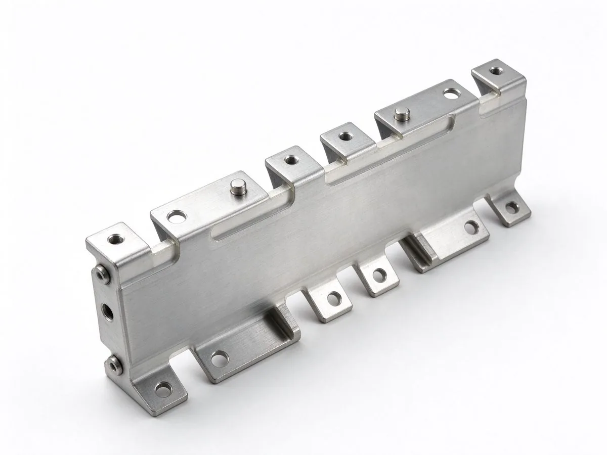
Higher switching speeds from SiC MOSFETs and modern IGBTs are pushing the DC-link busbar t
Read article
Daniel Richter is the chief electrical engineer at SHANYUAN Laminated Busbars, with 15 years in laminated busbar design and current-carrying systems. He leads electrical dimensioning, DC-link layout and thermal simulation for power converters, EV platforms and HVDC stations, and holds an M.Sc. in El
Send the current profile, voltage class and terminal types — our engineers reply within one business day.