Silicon carbide entered its scale-up phase in 2026. Single-crystal SiC substrates are on track to reach USD 1.8–2.2 billion by the end of the year (market forecasts published October 2026), 8-inch wafer conversion is expanding at 26–30% CAGR into the next decade, and data-center power electronics has joined automotive as a second demand pillar. For the engineers who build the modules and the systems around them, the interesting consequence is electrical: faster-switching SiC modules make the DC-link interconnect — the busbar — more electrically critical, not less, at every step of the scaling curve.
Silicon carbide entered its scale-up phase in 2026. Single-crystal SiC substrates are on track to reach USD 1.8–2.2 billion by the end of the year (market forecasts published October 2026), 8-inch wafer conversion is expanding at 26–30% CAGR into the next decade, and data-center power electronics has joined automotive as a second demand pillar. For the engineers who build the modules and the systems around them, the interesting consequence is electrical: faster-switching SiC modules make the DC-link interconnect — the busbar — more electrically critical, not less, at every step of the scaling curve.
Three market data points frame 2026. The global single-crystal SiC substrate market is projected to reach USD 1.8–2.2 billion by the end of 2026, with 200 mm wafer expansion unlocking 26–30% CAGR to 2031 (industry forecast published via GlobeNewswire, October 2026). The 8-inch SiC substrate segment alone is estimated at USD 1.45 billion in 2026 — about 23% of the overall substrate market — growing at a projected 14.5% CAGR to 2035 (Global Growth Insights, September 2026). And the 8-inch SiC wafer market, measured at USD 285.4 million in 2026, is forecast to multiply to USD 4.17 billion by 2035 at a 34% CAGR (Morgan Reed Insights, October 2026).
The direction is unambiguous: capacity is shifting from 150 mm to 200 mm platforms, which lowers cost per die and widens the addressable market — the same economics that drove silicon's 8-inch era.
Moving to 200 mm wafers cuts the cost per mm² of SiC die materially — roughly 1.7× more area per wafer — and the device-level benefit compounds through the module: more die per substrate, lower package cost per amp, and headroom for the die shrinks that follow. Yole Group's Power SiC 2026 report frames the conversion as the central technology trend of the year: wafer suppliers' 200 mm status, lower kerf losses, and reduced bowing are the supply-side levers.
For system builders the effect is a falling cost per ampere of fast-switching capability, which pulls SiC into applications where the silicon/IGBT incumbent had a cost advantage — and each new application inherits the interconnect problem.
Automotive (traction inverters, onboard chargers) remains SiC's largest market, but 2026 research points to data-center power as the fast-growing second pillar: 2026 market analyses put SiC and GaN data-center power growth CAGRs near 29.5% and 46.3% respectively (LimChip synthesis of Yole-type estimates, August 2026). The AI-server power chain — PSU, DC-DC stages, 48 V bus, VRM — is adding SiC where efficiency and density pay.
Our 800 VDC data-center article covers the rack-level power architecture; this article focuses on the module-level consequence: data-center power stages switch fast, carry high current, and are built inside dense racks where loop inductance and thermal budget are scarce.
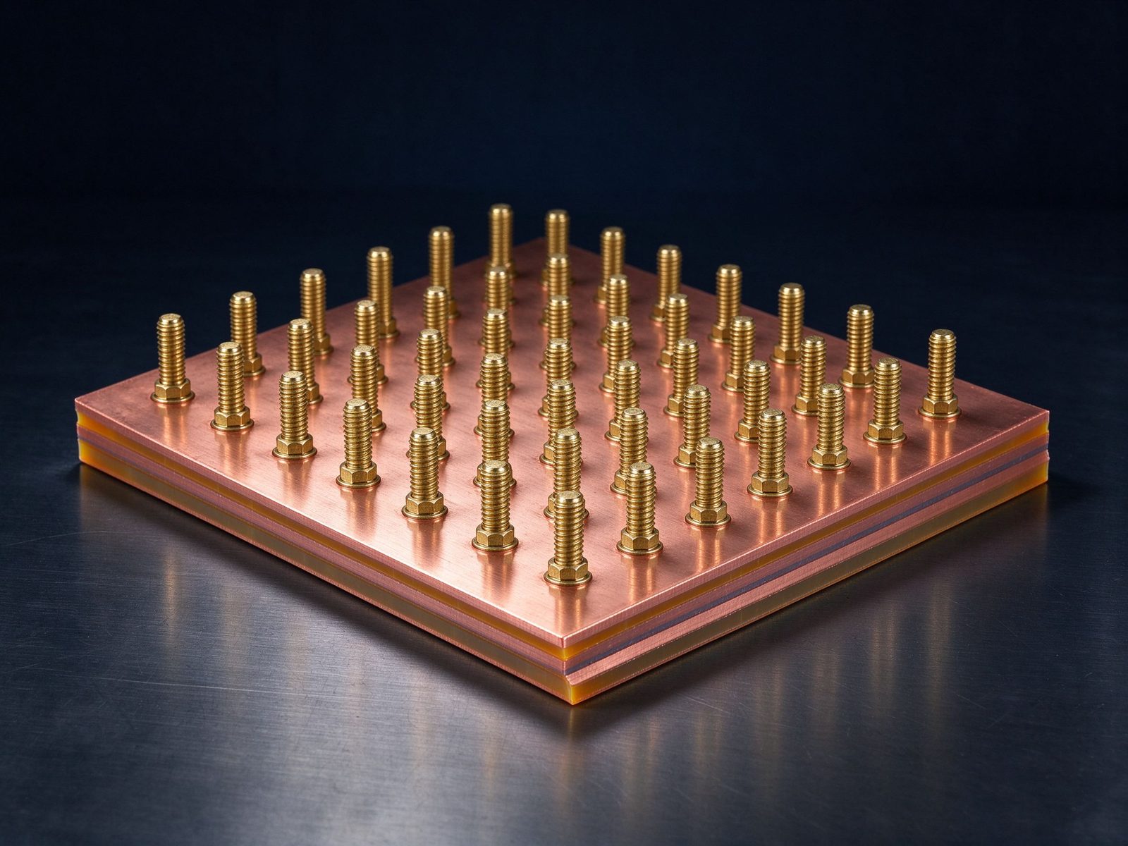
SiC's advantage — switching speed — is also its electrical stress: higher dv/dt and di/dt amplify the commutation-loop inductance problem, V_spike = L × di/dt. A module switching 600 A at tens of V/ns can convert 10 nH of loop inductance into a meaningful overvoltage spike; 30–50 nH (typical of cable or braid interconnects) becomes a reliability event.
The mitigation is geometric: a laminated busbar places the DC+ and DC− planes face-to-face, canceling loop area and holding inductance in the tens of nanohenries — the same physics our SiC/IGBT DC-link design guide quantifies for traction and industrial inverters.
2026 SiC module packaging continues its migration to multi-die, higher-current formats: larger modules with multiple parallel die, direct-copper-bonded substrates, sintered-silver die attach, and copper wire or clip interconnects. The module's DC terminals are increasingly blade or press-fit geometries designed to mate with a laminated busbar or PCB power plane rather than ring terminals and cables.
The trend is friendly to laminates: every ampere now flows through a planar interface, and the busbar design must match the module's terminal pattern precisely — a tolerancing problem covered in our fabrication tolerances guide.
Engineering budgets in 2026 designs: traction inverter DC-links specified at 5–15 nH total commutation loop; data-center and solar stages at 10–20 nH; module datasheets increasingly publishing a recommended maximum external loop inductance. Achieving these numbers requires the capacitor–busbar–module stack to be designed as one loop, with the laminate's layer spacing, terminal placement and current return path all contributing.
Measurement matters too: loop inductance is verified by double-pulse testing or impedance analysis, and the test fixture's contribution must be subtracted — a discipline we document with every power electronics busbar deliverable.
More SiC amps per cubic meter means the DC-link busbar must reject heat without shadowing the module's cooling path. Conductor cross-section is set by the temperature-rise budget (see our ampacity method), dielectric thickness is a thermal resistance in series with the die's heat path, and the terminal plane conducts heat between the module baseplate and the DC-link capacitors.
In 2026 data-center and traction designs, the common specification is a 30–40 K rise budget on the laminate at rated current, with the thermal check run on the assembled stack rather than the bare conductor.
SiC's voltage capability (1,200 V, 1,700 V and higher devices) is being used: 800 VDC bus architectures in data centers and commercial vehicles, 1,500 V solar DC-links, and 1,000–1,500 V battery systems. The DC-link laminate must satisfy IEC 60664-1 dimensioning with its 1.5× DC factor for insulation withstand, and partial-discharge screening increasingly appears in specifications for the 1,000 V-plus class.
The dimensioning method — CTI material groups, pollution degrees, creepage tables — is detailed in our creepage and clearance guide; the practical consequence is thicker dielectric build-ups and Nomex or epoxy-DLF constructions at the higher voltage class.
SiC demand in 2026 concentrates in three segments: EV traction and onboard charging (the volume base), solar and energy-storage PCS (where 1,500 V platforms favor SiC), and data-center power (the fastest-growing, smallest base). Each has a distinct busbar signature: traction uses low-inductance, high-vibration-tolerant laminates with welded or blade terminals; solar and ESS use 1,500 V-class laminates with high current density; data center uses compact, high-frequency laminates inside rack power shelves.
Our application pages document these variants, and the 2026 energy storage market article published today quantifies the storage-side demand context.
The 2026 SiC supply chain is consolidating around the 200 mm platform and its material suppliers. For busbar and interconnect suppliers the relevant signals are qualification-driven: module builders qualifying laminates to their thermal-cycling, vibration and partial-discharge requirements, with full material traceability and test records per lot. The quality system we run is built around exactly those deliverables.
Plating remains part of the qualification: tin on standard contact faces, silver where the interface sees high current density or repeated mating — the trade is quantified in our plating and corrosion guide published today.
The AI-server PSU chain in 2026 — 3.3 kW to 8 kW+ rectifiers, 48 V intermediate buses, VRM stages at sub-1 V — is the clearest example of SiC entering a formerly silicon-dominated segment. Near-load stages are DrMOS/SPS territory, but the front-end rectifier and the DC-DC stages increasingly use SiC (and GaN) where efficiency at high frequency pays for itself. Each stage has its own interconnect: the PSU's internal busbar carries hundreds of amps at 48 V, and the rack power shelf distributes current through busbars to the compute shelves.
The 800 VDC rack article and our data center power busbar overview map that chain end to end.
Verifying a SiC power stage means verifying the commutation loop: double-pulse testing measures switching energy and peak voltage at rated current, and the test result depends on the fixture's loop inductance as much as the module's. Busbar suppliers who provide inductance-verified parts (measured, not calculated) shorten the customer's bring-up cycle and prevent the classic 'module burns out on the test bench' failure.
Beyond electrical testing, the insulation testing guide covers the hipot, IR and PD screening that 1,000 V-plus laminates require before shipment.
SiC's falling cost per amp pulls against a second 2026 cost pressure: copper at record prices. With LME copper at historic highs, module and system builders ask whether aluminum conductors can serve the DC-link — the trade (resistivity, cross-section, thermal, plating) is quantified in our aluminum versus copper article. The short answer for fast-switching SiC stages: conductivity and loop geometry favor copper laminates; aluminum appears where weight or cost dominates and the loop can be sized up.
The decision is per-application, and the calculation method is public.
Extrapolating the 2026 curves: 8-inch SiC substrates double or triple by 2028–2029, data-center power keeps growing at the fastest rate, and 1,700 V-class devices push DC-link voltages up in grid and storage applications. For interconnects, that means more current per module, higher voltage classes, and tighter loop budgets — all laminate-friendly trends, and all requiring the fabrication and tolerance discipline that scales with volume.
The suppliers who win the platform qualifications in 2026 are the ones who ship 2028 volume, which is why we treat every qualification sample as a production part.
SiC in 2026 is a story of scale — $2B substrates, 8-inch conversion, data-center demand — but the electrical story is speed. Faster switching converts loop inductance into voltage stress, and the DC-link busbar is the component that either absorbs that stress or amplifies it. The module gets the press release; the laminate gets the voltage spike.
When you evaluate SiC for your next inverter, PSU or traction stage, run the interconnect through the same scrutiny as the die: loop inductance budget, temperature-rise calculation, insulation coordination, and test verification. Our engineers do that on every custom busbar inquiry — send the platform parameters and get the laminate design back, with the numbers attached.
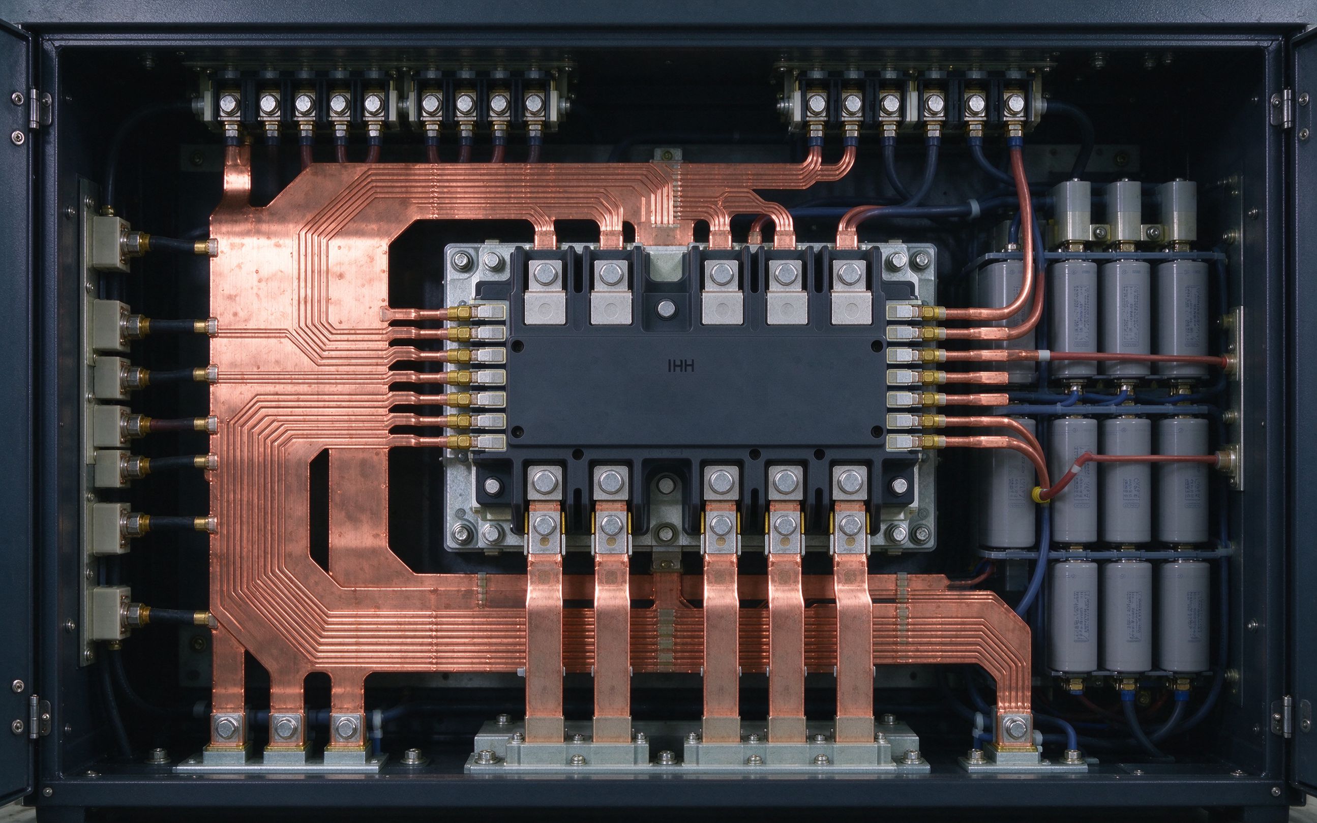
The inverter that dominated 2026's solar tenders is no longer a small box: 300 kW-plus str
Read article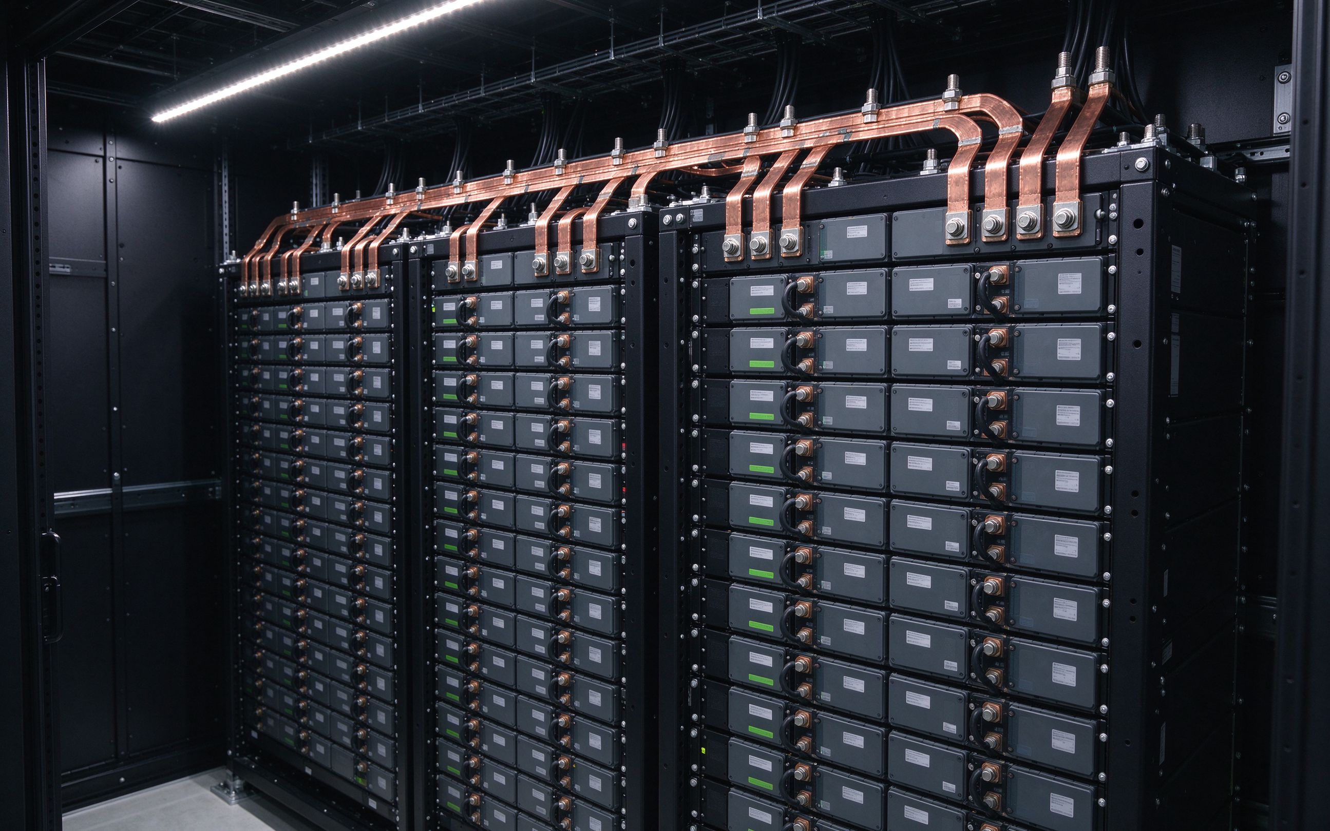
AI racks move from 140 kW to 1 MW by 2027, and the industry answers with 800 VDC distribut
Read article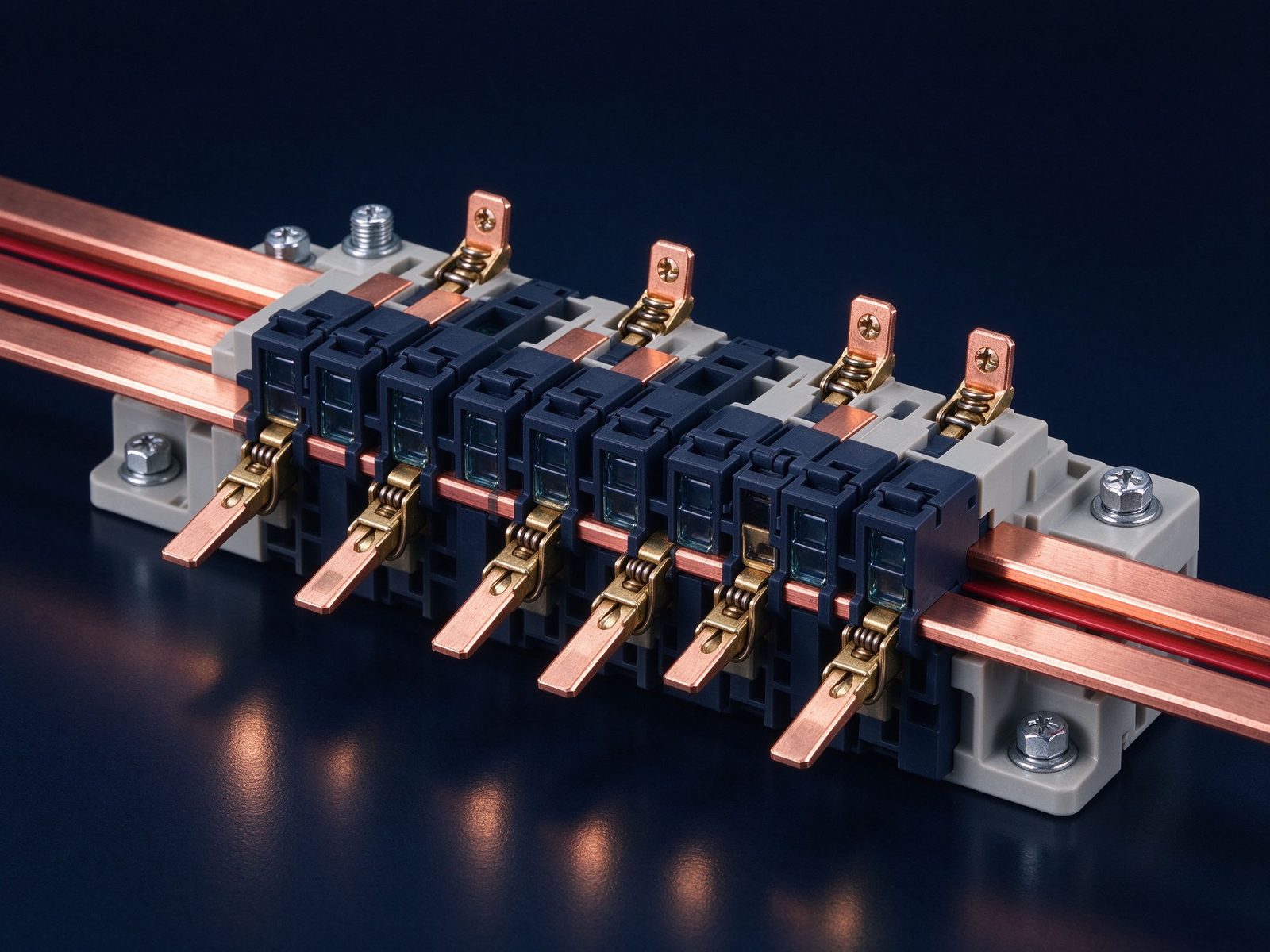
A short circuit is the busbar's worst moment: tens of kiloamps peak, forces in kilonewtons
Read articleSend the current profile, voltage class and terminal types — our engineers reply within one business day.