Laminated busbar failure modes are rarely electrical — they are dimensional. A hole position that drifts 0.3 mm misaligns the terminal stack and the bolt, a bend angle that opens 1.5° twists the conductor out of the mounting plane, and a burr on the conductor edge punctures the dielectric during lamination. This guide converts the DFM rules we enforce in our stamping and bending shop into numbers engineers can put on a drawing: the tolerances, the radii, and the cost of precision.
Laminated busbar failure modes are rarely electrical — they are dimensional. A hole position that drifts 0.3 mm misaligns the terminal stack and the bolt, a bend angle that opens 1.5° twists the conductor out of the mounting plane, and a burr on the conductor edge punctures the dielectric during lamination. This guide converts the DFM rules we enforce in our stamping and bending shop into numbers engineers can put on a drawing: the tolerances, the radii, and the cost of precision.
On a busbar, dimensions are not just fit — they are electrical. The hole pattern sets the joint contact area and the torque distribution across the connection; the flatness of the mating face sets the effective contact surface at a bolted joint; the edge condition determines whether the dielectric survives lamination; and the bend geometry sets the conductor's path through the enclosure and its clearance to neighboring parts.
This is why our DFM review treats tolerance as a first-order electrical parameter: a part that meets its ampacity calculation but misses its hole pattern by half a millimeter is a failed part, not a cosmetic one. The DFM checklist article covers the review structure; this article quantifies the numbers.
Commercial busbar fabrication runs to ISO 2768, the general-tolerances standard. Part 1 (linear and angular dimensions) defines precision grades fine (F), medium (M), coarse (C) and very coarse (V); Part 2 (geometrical tolerances) defines classes H, K and L. The industry-standard combination is ISO 2768-mK: medium linear tolerances with the K geometrical class, stated in the drawing title block.
Published practice for copper busbars under ISO 2768-mK: linear dimensions held to ±0.2 mm for lengths up to 150 mm, ±0.3 mm up to 600 mm; bend angles to ±1°; hole positions to ±0.15 mm for standard punching. These are the numbers a drawing gets 'for free' without calling out individual tolerances — and the baseline against which precision options are priced.
The standard envelope: linear dimension ≤ 150 mm, ±0.2 mm; ≤ 600 mm, ±0.3 mm. Hole position from standard punching, ±0.15 mm; CNC punching or machining improves this to ±0.05 mm. Hole diameter, ±0.1 mm standard, ±0.05 mm precision. The precision upgrades carry real costs — published industry figures put precision hole positioning at roughly €0.50–€1.00 per hole additional, and precision classes add 15–50% to part cost depending on the feature set.
For a battery module busbar with a 4-stud terminal pattern, the cumulative benefit of ±0.05 mm hole position is a bolt pattern that aligns first time with the module fixture. For a long distribution bar with a dozen mounting holes, standard ±0.15 mm is usually sufficient. The decision rule is alignment-criticality: terminal patterns and mounting to mating hardware get precision; clearance holes and non-functional features get standard.
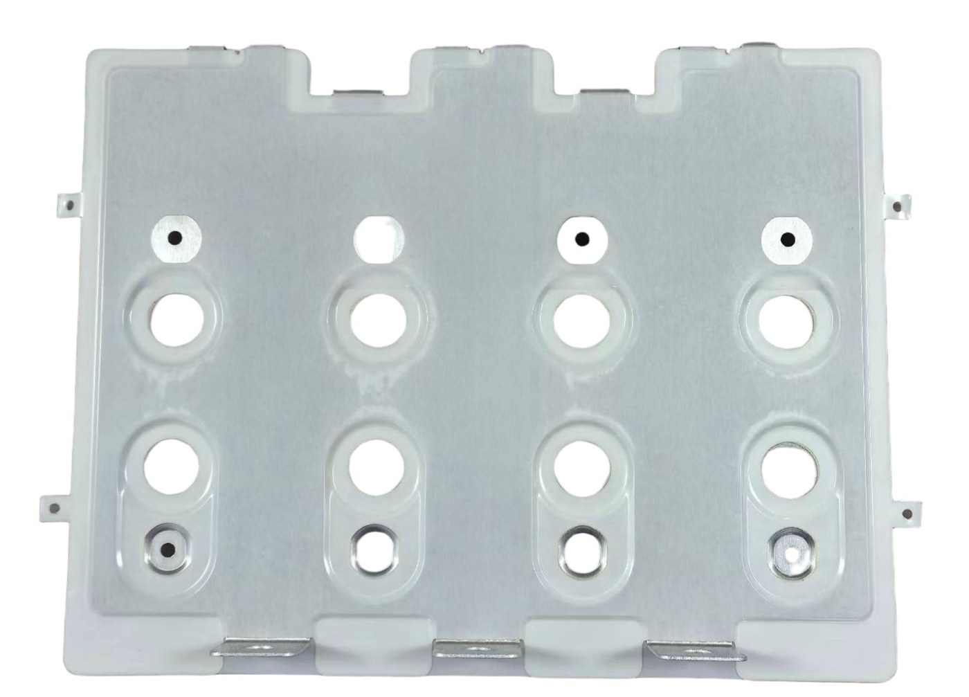
The minimum internal bend radius is set by the material, not the preference. For C1100 ETP copper and C260 brass, the published minimum is 0.5× material thickness — the same class as mild steel. Stainless steel and 5052-H32 aluminum need 1×T; 6061-T6 aluminum needs 3×T. Bending tighter than the material allows cracks the bend line — a failure that cannot be reworked, only scrapped.
With a K-factor range of 0.35–0.45 for copper, the bend allowance calculation must use the actual tooling and material temper; the difference between K = 0.35 and K = 0.45 across several bends can accumulate to a millimeter or more of flat-pattern error, which is exactly where the final hole position goes wrong.
Bend angle tolerance with standard press-brake tooling is ±1°. Precision forming with CNC control and calibrated tooling achieves ±0.5°, at a documented cost increase of 25–35% over standard. Angular tolerance matters because a busbar that mounts to a three-dimensional structure — an inverter DC-link with studs at two levels, a battery pack with terminal bars crossing the module — accumulates angular error into misalignment at every interface.
Copper is a springback-prone material: the bend relaxes after forming, and the compensation must be set per material lot and tool condition. The shop practice is to over-bend by the measured springback angle, verify on first article, and lock the compensation into the CNC program. If the drawing calls ±0.5° without acknowledging springback, the parts will fail even though the tooling is capable.
A hole placed too close to a bend line deforms as the metal stretches or compresses around the bend: the hole becomes oval and the edge cracks. The design rule is to keep hole edges at least 2× material thickness from the bend line (some shops run 2.5×T for thicker material). When a hole must sit close to a bend — a terminal hole right at the fold of a U-bend — the options are to bend first and punch after, or to accept the distortion and open the hole to tolerance.
This is one of the most common DFM corrections we make on incoming drawings, and it is free to fix before tooling: move the hole, or re-sequence the process.
For a laminated busbar, the conductor edge condition is a dielectric requirement, not a cosmetic one. A burr or sharp edge on the punched conductor concentrates electric field and can puncture the PET or Nomex layer during lamination or in service under voltage — the same edge-stress mechanism that insulation coordination and partial discharge control are designed against.
The manufacturing measures are: sharp-edge deburring (vibratory or abrasive), edge radiusing or chamfering where the conductor sees voltage stress, and burr-direction control so any residual burr faces the non-critical side. Our stamping shop specifies edge condition per part class, and the inspection records the edge state on the first article alongside the dimensions.
A bolted busbar joint transfers current through the mating faces; flatness controls how much of the face actually contacts. A bowed or twisted bar contacts on a fraction of its area, raising contact resistance and creating the hot spot that fails temperature-rise tests. Coining or spot-facing the contact area is the standard fix: it produces a controlled, flat contact zone around the hole with a defined surface finish.
The tolerance callout for a joint face is a flatness or coining specification, not just a surface-roughness note, and it belongs on the drawing at the terminal pattern. The terminal connection guide covers the torque and surface practice that turns a flat face into a stable joint.
Tin plating thickness (our standard surface, typically 3–10 µm on contact areas) has its own tolerance and its own failure mode: too thin, and the oxide protection and solderability degrade; uneven, and the contact resistance varies across the joint. Plating is specified by thickness range, not 'tin plated', and measured by X-ray fluorescence or cross-section on qualification parts.
Plating also interacts with tolerances: a thick plating on a hole changes the effective hole diameter for the bolt, and plating buildup at edges can affect the fit of insulating sleeves. The design rule is to specify the plated dimensions and the plating thickness separately, and to inspect both.
When stamped conductors are laminated into a multi-layer busbar, the alignment of the layers relative to each other — hole-to-hole concentricity across the stack — is a laminated-part tolerance that has no bare-bar equivalent. Misaligned layers mean misaligned stud holes and a terminal pattern that fights the module fixture. The lamination tooling uses pilot holes or datum features punched into each layer, and the stack alignment is a documented first-article dimension.
This is where the stamped part's tolerance budget interacts with the lamination process: layer-to-layer offset, dielectric registration and the final stud position all contribute to the terminal pattern the customer sees. The manufacturing process article describes the lamination sequence; the tolerance responsibility is shared between the stamping and lamination steps.
Precision is a budget decision. Published industry figures for copper busbar fabrication: linear precision (±0.1 mm vs ±0.2 mm) adds ~15%; precision hole position (±0.05 mm vs ±0.15 mm) adds ~50% on the feature; precision bend angle (±0.5° vs ±1°) adds 25–35%; precision hole diameter adds ~25%. Over-specifying ISO 2768-f (fine) when medium would suffice adds 20–25% to total part cost through slower programs and increased inspection, and anything tighter adds 40–80%.
The engineering discipline is to call precision only where the interface demands it: terminal patterns, mating hardware, and laminate datum features. Clearance holes and non-functional dimensions stay at standard. This is the same logic as the design guide — specify what the function requires, nothing more.
A busbar drawing that survives DFM review carries five explicit callouts: (1) 'GENERAL TOLERANCES: ISO 2768-mK' in the title block; (2) precision callouts on the terminal-pattern hole positions (e.g., position tolerance Ø0.1 mm at the stud pattern); (3) minimum bend radius stated per bend (0.5×T for C1100); (4) flatness/coining callout at joint faces; and (5) plating thickness range on contact areas. Without these, the shop defaults to its standard envelope, which may or may not be what the joint requires.
Ambiguity costs twice: once in scrap, once in schedule. The five callouts are cheap insurance, and they are the first thing our DFM review checks.
Inspection follows the tolerance callouts: CMM or optical measurement of the terminal pattern and hole positions; bend-angle verification by fixture or profile projector; thickness and flatness checks on joint faces; and XRF measurement of plating thickness on qualification parts. The inspection frequency maps to the risk: terminal patterns on every first article and at defined lot intervals, clearance features on first article only.
Documentation is part of the deliverable — our quality records attach the dimensional report to each lot, so the customer's incoming inspection can confirm the numbers rather than trust them. The quality system page describes the framework.
The recurring errors we see: calling bend angle ±0.5° without springback compensation; placing holes within the bend zone; specifying plating thickness without a range; tolerancing every dimension fine when only the terminal pattern needs it; and omitting the edge-condition note on a voltage-class part. Each has a concrete cost: the springback part is scrapped; the bend-zone hole distorts; the unmeasured plating fails a joint test; the over-tolerance quote comes back 20% high; the sharp edge fails a PD test.
All five are drawing-time fixes. None of them require exotic capability — they require the numbers to be on the drawing, which is what this guide is for.
Every tolerance decision in this article is checked in the DFM review we run on every inquiry before tooling: material and temper, bend radius against the drawing, hole-to-bend clearance, edge condition, plating specification, laminate datum alignment, and the precision-versus-cost balance. The review output is a marked-up drawing and a tolerance rationale, so the customer sees the decisions, not just the part.
The EU battery program context adds one more layer: the documentation and design-for-recycling requirements of the battery passport chain rely on the same part-level data discipline. Send your drawing to our engineering team — the DFM review, including the tolerance callouts, is part of every quotation.
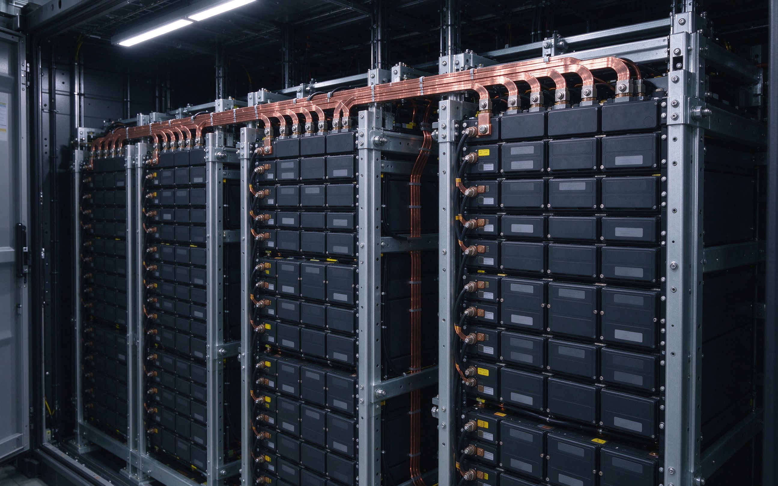
The EU Battery Regulation (2023/1542) makes the battery passport mandatory on 18 February
Read article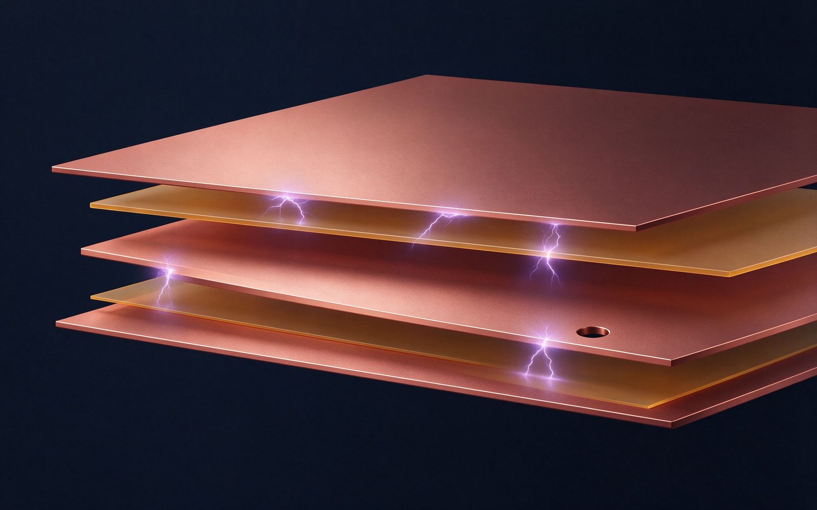
A busbar fails across a surface long before it fails through its insulation if the creepag
Read article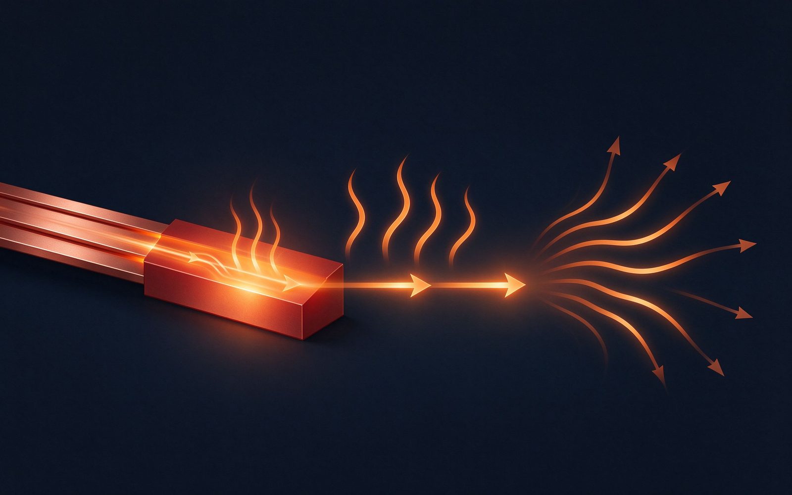
A busbar's rating is not a lookup — it is a calculation. Temperature rise is the real limi
Read articleSend the current profile, voltage class and terminal types — our engineers reply within one business day.
Send drawings, current ratings and voltage class — DFM feedback and a quotation within one business day.