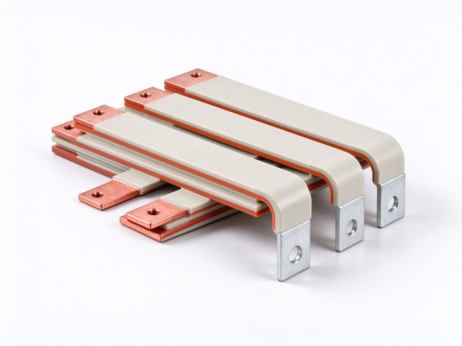
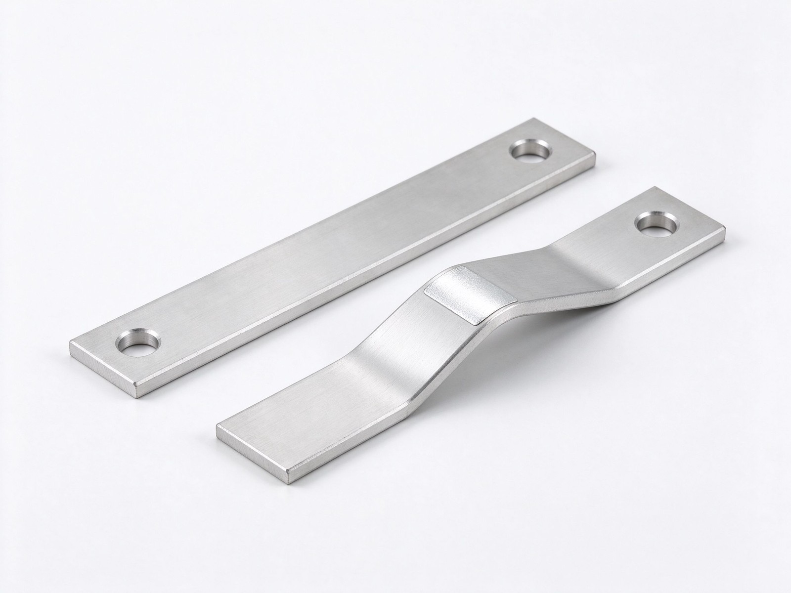
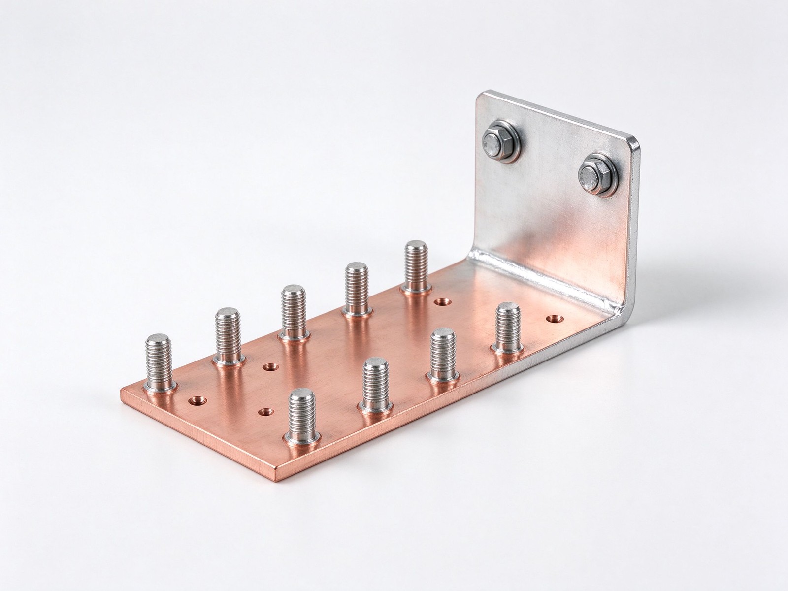
Copper or brass PCB stiffener busbar that routes high current to targeted board zones while bracing the assembly against shock and vibration.
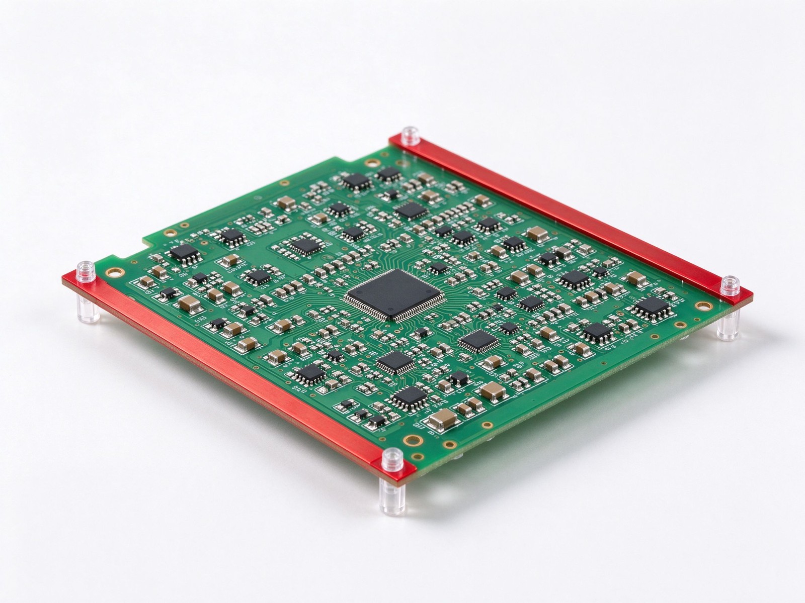
Product imagery: factory photo plus studio renders. The exact geometry, layers and terminals of your part follow your drawing.
Final values follow your drawing — this is the standard configuration of the family.
| Parameter | Value |
|---|---|
| Conductor | C11000 copper or brass (Cu-Zn) bar |
| Board function | High-current routing + mechanical stiffening |
| Mounting | Transparent standoffs, perpendicular or back-panel flush |
| Plating | Tin, tin-lead, lead, or dielectric powder coat |
| Current path | Routed only to target components per layout |
| Edge finish | Rounded, deburred board-safe edges |
| SKU | SY-CM-316 |
Key characteristics of this product family.
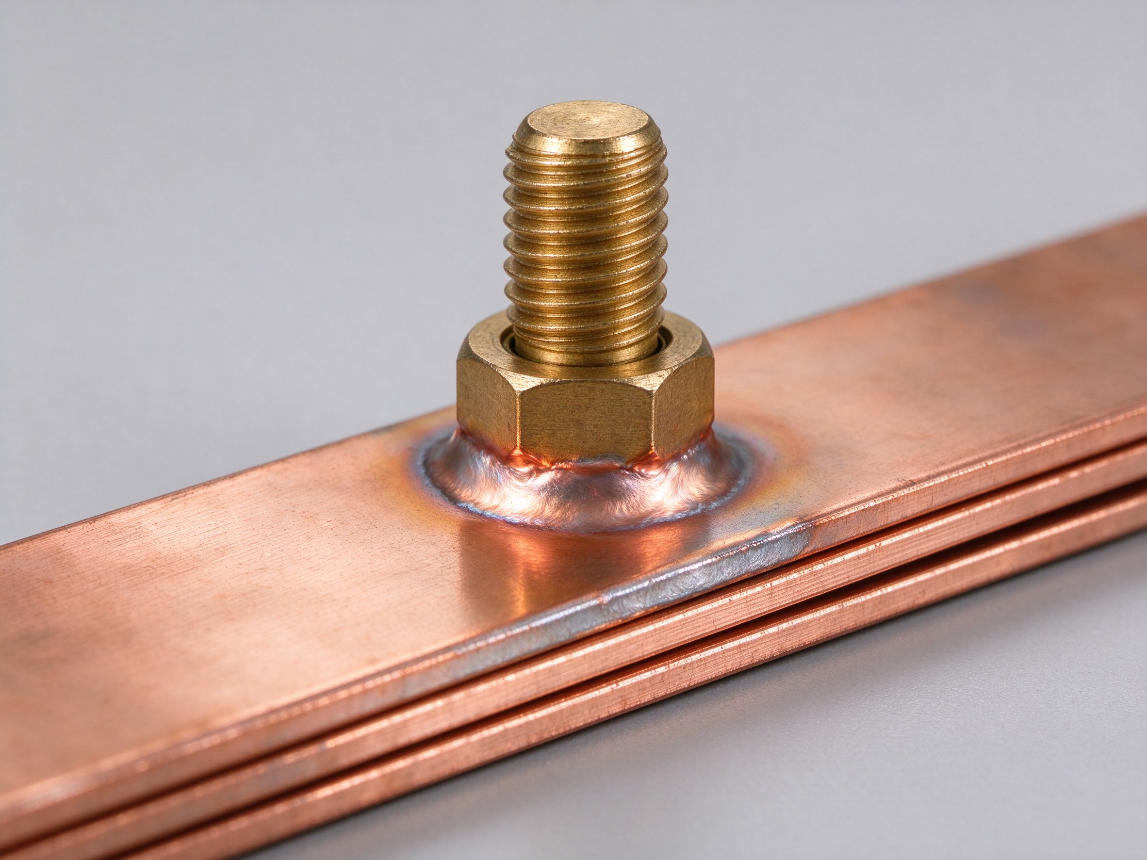
A PCB busbar stiffener is a custom copper or brass bar mounted across a printed circuit board to do two jobs at once: carry high current to the few zones that actually need it, and mechanically brace the board so the laminate and solder joints stay within their stress limits.
As board current demand grows, many designs respond by thickening the copper layer across the entire board. That adds weight everywhere, loads the dielectric and raises cost - when only a handful of traces need the extra metal. A stiffener concentrates the current path where it is required without penalising the rest of the board.
Beyond the current path, the stiffener improves reliability under mechanical stress. It reduces shock and vibration effects on the board, its components and the solder joints, which matters in traction drives, industrial controls and battery systems that live through continuous vibration.
Plating is selected to match the battery chemistry the board serves. Tin-plated stiffeners are typically paired with powder-coated bars for sealed battery applications, while lead or tin-lead alloy plating suits flooded wet cells. Where a PCB needs multi-circuit or multi-layer current routing, a laminated busbar can serve as the stiffener, and powder-coated bars rigidify the board while shielding it from current leakage and environmental moisture.
Thickening copper across an entire PCB adds weight and cost to every square centimetre of laminate, but a stiffener adds metal only along the current path. The board keeps its normal copper weight everywhere else, so the dielectric carries less mass and the assembly stays within its mechanical limits. Where a zone still needs more metal, our multi-layer laminated busbars spread current across stacked conductors, and our thermal management guidance covers the heat these paths generate.
Stiffener plating follows the electrolyte chemistry of the battery pack:
For corrosion and leakage protection on any bar shape, see our dielectric epoxy coating service.
Send the board layout with the high-current zones marked, the required current per zone, and the available standoff height. Our engineers map the current path, set the bar cross-section and hole pattern, and confirm the plating for your battery chemistry - all as part of the custom busbar design service with a DFM review before tooling. Quotes typically return within one business day.
A PCB busbar stiffener doubles as the high-current path and the board brace, so the bar alloy is chosen for both conductivity and mechanical stiffness. The table gathers the stock-alloy ratings for the two metals we machine stiffeners from.
| Board-Bar Material Item | Typical Data | Assembly Note |
|---|---|---|
| Copper option (C11000) | 100% IACS, half-hard temper | Best conductivity, zones above 50 A |
| Brass option (C36000) | ≈ 28% IACS, free-machining | Stiffest brace, lower current duty |
| Bar width range | 6–40 mm typical | Cut from strip, milled to width |
| Bar thickness range | 1.5–6 mm typical | Sets board stand-off height |
| Plating, sealed cells | Tin 5–15 µm, powder coat option | Sealed-cell VRLA, AGM, gel duty |
| Plating, flooded cells | Tin-lead or lead flash | Wet-cell corrosion resistance |
| Hole array pitch | 2.54 / 5.08 / 7.62 mm grid | Matches PCB via and stand-off drills |
| Thermal expansion | Copper ≈ 17 × 10⁻⁶ /K | Close to FR-4, low shear stress |
| Green declaration line | RoHS and REACH compliant per batch | Material-level note per policy |
Strip mill certificates and plating-thickness records are issued per batch on request. A PCB stiffener bar copper brass choice usually comes down to current: brass when the job is mostly bracing, copper when the zone carries real current. Half-hard temper keeps the bar flat after milling, which matters on a board that must slip under a stiffener bracket without spring. The brass option machines to tighter hole tolerances, which is why it is preferred where the hole array has to line up with press-fit or solder-in pins. Guidance on the sealed battery PCB stiffener plating question appears in our plating finishes note, and board-level heat in our resource on thermal-rise guidance.
Sizing a PCB stiffening busbar vibration solution is a three-step mapping exercise: mark the zones, size the section, drill the array. The table pairs board-zone currents with the bar cross-sections we usually lay out.
| Stiffener Bar Size | Current Capacity | Typical Hole Array |
|---|---|---|
| 10 × 2 mm | 40–60 A typical | M3 on 5.08 mm pitch |
| 15 × 3 mm | 80–120 A typical | M3 / M4 on 5.08–7.62 mm |
| 20 × 3 mm | 120–180 A typical | M4 on 7.62 mm pitch |
| 25 × 4 mm | 180–260 A typical | M4 / M5 on 7.62–10 mm |
| 30 × 5 mm | 260–350 A typical | M5 on 10 mm pitch |
The capacities above are typical free-air estimates; board-mounted parts run hotter because the FR-4 beneath them traps heat, so derate toward the low end where the board is sealed. Keep the bar on the outer layers where possible: buried stiffener runs are hard to inspect and rework. Where the zone current exceeds 200 A, step the bar up one size rather than forcing more height under the stand-off, because board flex near the connector is the failure mode to design out. The current-density basis for the table is the same method behind the busbar ampacity chart, and the vibration context in our note on bolted-joint and vibration practice. Send the zone map and we return a layout for DFM review. Tell us the board thickness and connector location; the stiffener ends usually land beside the connector rather than across the whole board.
Where this busbar configuration earns its place.
Where this busbar configuration earns its place.
Where this busbar configuration earns its place.
Where this busbar configuration earns its place.
Where this busbar configuration earns its place.
Where this busbar configuration earns its place.
Your drawings reach the engineers who build the part.
Design risks flagged when changes are cheap.
Test records per lot, CoC and PPAP on request.
Drawing to delivered production parts, one supplier.
From spec review to shipped, tested parts — one accountable supplier.
Straight answers from the engineering team.
Every SHANYUAN busbar is custom, but the power circuits they connect recur across markets. Three typical ones — send us yours and we will point to the right stack-up.
Tight, low-inductance links between the battery source and traction inverters, fully edge-sealed for 400–800 V platforms.
Commutation-loop connections from DC-link capacitors to IGBT bridges, designed against switching overshoot V = L × di/dt.
Converter DC links built for rising bus voltages toward 1500 VDC, with creepage and partial-discharge margins included.
Construction, dielectric selection and current capacity basics.
Read the busbar design guideLayers, terminals, dielectrics and mounting are all configurable. Send us your spec for DFM review and a quotation within one business day.