A conventional transformer isolates by geometry: windings separated by insulation and oil or resin. A solid-state transformer isolates by switching, and in between sits a medium-voltage DC link fed by a busbar that must hold 10 kV, carry hundreds of amps of ripple current, and stay quiet at every switching edge. That is a different component from the 800 V DC-link bar the industry already knows how to build.
A conventional transformer isolates by geometry: windings separated by insulation and oil or resin. A solid-state transformer isolates by switching, and in between sits a medium-voltage DC link fed by a busbar that must hold 10 kV, carry hundreds of amps of ripple current, and stay quiet at every switching edge. That is a different component from the 800 V DC-link bar the industry already knows how to build.
This page is an annual rolling data page: the 2026 edition, refreshed once a year as new market data is published.
A solid-state transformer converts medium-voltage AC to an internal DC link, then back to AC or DC at the load. The MV front end typically operates at 10 to 13.8 kV, and the DC link sits at a correspondingly high potential, fed by SiC or GaN devices switching at tens of kilohertz.
Three consequences follow for the busbar. Clearance and creepage are set by kilovolts rather than hundreds of volts. Partial discharge becomes a first-order design constraint because a void that is harmless at 800 V will erode insulation at 10 kV. And stray inductance, already important in a SiC converter, now interacts with a much higher dV/dt and a longer current path.
The result is a component that looks like a laminated bar but behaves like an insulation system. Mechanical thickness, film selection and edge geometry matter more than the copper cross-section, and the qualification regime is closer to high-voltage switchgear than to an inverter DC link.
At 10 kV, clearance in air is no longer a matter of a few millimetres, and the presence of a grounded enclosure wall changes the field distribution. A design that places the bar at the minimum tabulated distance may pass a hipot and still discharge in service, because the table assumes a uniform field that the actual geometry does not provide.
Practical designs add margin at the interfaces: rounded conductors rather than sharp edges, solid insulation or potting at the highest-field regions, and a physical barrier between the DC link and the low-voltage compartment. Each of these is a busbar-level decision, not a panel-level afterthought.
The interface problem is harder in an SST because the MV compartment and the LV compartment sit close together for cable and cooling reasons. A laminated bar crossing that boundary must be specified with the transition geometry, not only the conductor.
Our clearance and creepage note covers the field-based approach; the difference here is the voltage class.
At medium voltage, a void in the insulation or a sharp burr at the conductor edge becomes a discharge site. The discharge does not cause an immediate failure; it erodes the dielectric, generates ozone and eventually produces a tree that punctures.
This is why SST busbars are specified with a PD limit rather than a hipot pass. Hipot proves the dielectric can survive a short overvoltage; PD measurement proves there is no site that will degrade over years. They answer different questions.
The test itself is sensitive to the environment: background noise, shielding and detector calibration determine whether a 5 pC reading is a defect or an artefact. A supplier claiming PD compliance without stating the background level and the standard used is not giving you evidence.
Our partial discharge testing note describes the bench arrangement and the pass criteria we apply.
For the design rules behind void-free laminates, see our partial-discharge-free busbar design guide.
In a SiC-based converter, the DC-link loop inductance sets the overvoltage at turn-off. At 10 kV, even a few nanohenries produce a spike that stresses both the device and the insulation. The busbar is the dominant contributor to that loop, so its geometry is part of the device protection, not only the power path.
Two design moves reduce loop inductance: bring the return path physically close to the forward path, and use multiple parallel layers so the current can spread. A four-layer stack with a thin dielectric between adjacent opposing layers can reach single-digit nanohenries, provided the terminal arrangement does not add a long shared path at the ends.
The counter-constraint is insulation: the thinner the dielectric, the better the inductance and the harder the PD requirement. That trade-off is the core design decision in an SST busbar, and it is resolved with material choice and field grading rather than with a single number.
The method is set out in our low-inductance design resource.
PET films that work well at 800 V are not automatically suitable at 10 kV, particularly under repetitive fast transients. The material choice has to consider dielectric strength, partial-discharge inception, thermal class and processing behaviour together.
Polyimide and Nomex offer higher thermal margins and better PD behaviour at elevated temperature; PET offers better cost and processability. Epoxy powder coating provides a conformal layer that reduces field concentration at edges and is often used in combination with film insulation rather than instead of it.
The failure mode to design against is not a single breakdown but cumulative degradation at an edge or a void. That means the material specification must include the processing conditions - lamination temperature and pressure - because a film bonded with entrapped air is a film with built-in voids.
Material selection logic is covered in the dielectric selection guide; the SST-specific addition is the MV qualification evidence.
SST busbars usually carry lower total current than a 1000 A inverter link, but the loss is concentrated: at the terminals, at the film-to-copper interface, and wherever the geometry forces current to crowd. Local hot spots drive PD inception and insulation ageing more than average temperature does.
This is why an SST busbar design is often evaluated with a thermal model rather than a single ampacity number. The question is not "how much current can this bar carry" but "what is the temperature at the highest-field point under the actual ripple current".
The practical design responses are generous terminal cross-sections, symmetric layer assignment and, where possible, moving the highest-field region away from the hottest one - which sometimes means accepting a slightly higher inductance to gain thermal margin.
Our thermal management resource covers the calculation approach; IGBT module busbar sets show how terminal geometry is handled in practice.
A qualification sequence typically runs: material and process review, sample build, dimensional and X-ray inspection, PD measurement at rated and overvoltage, thermal cycling, and a final PD re-measurement. The last step is the one that catches process problems, because cycling opens voids that a single measurement misses.
The evidence pack should state the PD limit, the test standard, the background noise, the voltage levels and the number of cycles. Without those, a "passed PD" statement cannot be compared between suppliers.
Programmes also need a change-control agreement: any change in film supplier, adhesive, lamination pressure or terminal geometry requires re-qualification. In an MV component that is not bureaucracy; it is the only way to keep the evidence valid.
If you are preparing an SST qualification plan, our team can review the busbar section against your converter topology through the contact form.
The commercial pull is coming from three directions: data centres with very high power density and a desire to remove low-frequency transformers from the power chain; fast-charging hubs where the footprint of a conventional transformer and its cooling is a constraint; and traction and marine systems where weight and volume dominate.
Each application imposes a different balance. Data centres care about efficiency and serviceability, so modular replacement and connectorised busbars matter. Charging hubs care about cost per kW and outdoor environmental robustness. Traction cares about vibration and thermal cycling.
All three share a requirement that is new to many busbar suppliers: the ability to deliver medium-voltage evidence, not only a good 800 V design. That capability is what separates a supplier that can support an SST programme from one that can only quote a prototype.
First, can you measure partial discharge, and what is your background noise? A supplier without a shielded PD bench cannot qualify an MV design, however good its lamination is.
Second, what is your process control for voids - film storage, lamination pressure record, edge preparation? Voids are made in process, not in design.
Third, what happens to the qualification when a material changes? If the answer is "we will test again", ask for the re-qualification plan and the notification clause.
A supplier that answers all three with documents is ready for a first article. A supplier that answers with confidence is not.
Start from the converter, not the busbar: define the DC-link voltage, the switching edge rate, the allowable overvoltage at the device, the PD limit and the thermal environment. Those five inputs determine the insulation thickness, the layer arrangement and the terminal geometry.
Then define the interface: where the MV compartment ends and the LV compartment begins, and who owns the clearance at the boundary. Most SST busbar problems that reach production are interface problems that were never drawn.
SHANYUAN builds laminated busbars for converter applications from 800 V to medium-voltage front ends, with in-house PD testing and a documented change-control process. Send the topology and the five inputs through our contact form and we will return a first-pass geometry and qualification plan.
Related: SiC DC-link busbars, low-inductance design and dielectric selection.
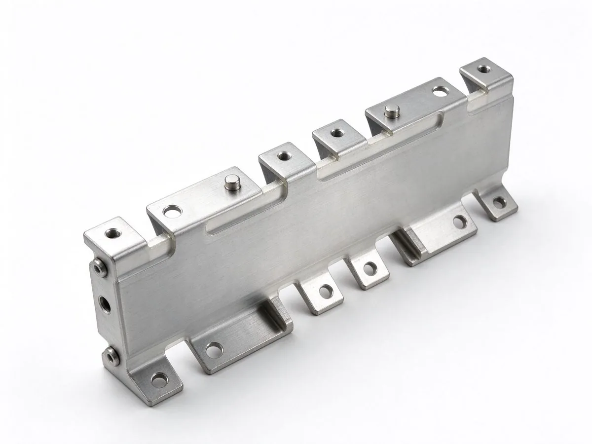
Higher switching speeds from SiC MOSFETs and modern IGBTs are pushing the DC-link busbar t
Read article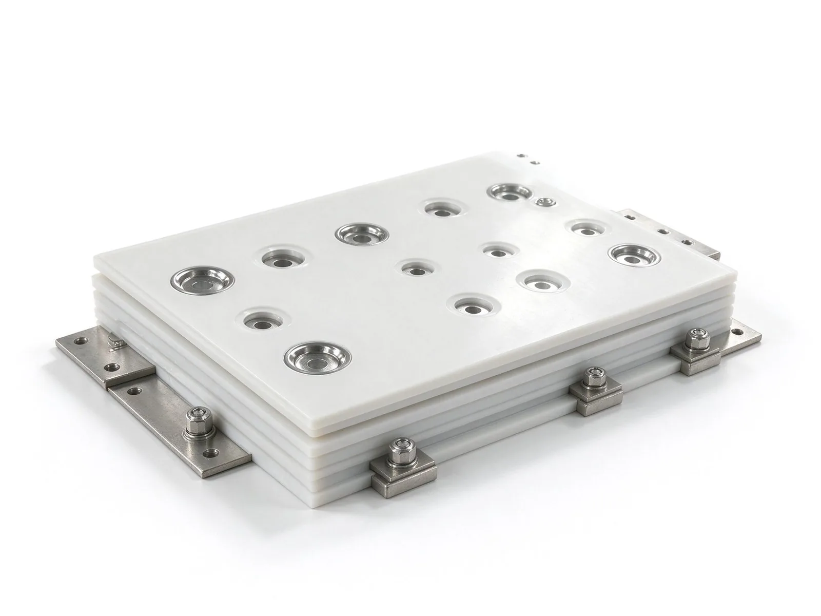
A busbar fails quietly when a void inside its insulation starts discharging. This guide co
Read article
PET, Nomex and DLF epoxy are the three dielectrics we laminate into SHANYUAN busbars every
Read article
Elena Vasquez is a power electronics application engineer with 10 years of experience integrating laminated busbars into EV inverters, charging systems and energy-storage PCS. She specializes in low-inductance DC-link design, EMC behaviour and converter packaging, and holds a B.Sc. in Electrical Eng
Send the current profile, voltage class and terminal types — our engineers reply within one business day.