Every power-electronics engineer knows that high-frequency current does not fill a conductor. The deeper truth is quantitative: the skin depth of copper at 20 kHz is about 0.47 mm, so a 6 mm-thick solid bar carries most of its switching-frequency current in the outer half-millimetre of each face. The resistance penalty is exponential in the high-frequency limit, and the proximity effect between adjacent conductors makes it worse. This guide gives the numbers, the mechanisms and the design rules - including why the laminated stack is the natural answer.
Every power-electronics engineer knows that high-frequency current does not fill a conductor. The deeper truth is quantitative: the skin depth of copper at 20 kHz is about 0.47 mm, so a 6 mm-thick solid bar carries most of its switching-frequency current in the outer half-millimetre of each face. The resistance penalty is exponential in the high-frequency limit, and the proximity effect between adjacent conductors makes it worse. This guide gives the numbers, the mechanisms and the design rules - including why the laminated stack is the natural answer.
The classical skin depth is delta = sqrt(2 rho / (2 pi f mu)), where rho is resistivity, f the frequency and mu the permeability. For copper at 60 Hz, delta is about 8.5 mm - a bar thinner than that carries current almost uniformly. At 20 kHz, delta falls to 0.47 mm (NovaSolver, 2026); at 100 kHz it is roughly 0.21 mm. Above a few kilohertz, the centre of a thick bar is electromagnetically dead weight: it carries no current, contributes no conductance and adds mass, inertia and cost.
The engineering conclusion is not to make bars thinner in general - it is to keep each conductor's thickness on the order of a couple of skin depths and to add surface where current actually flows. This is the same logic that makes transformer cores laminated rather than solid.
Where two parallel conductors carry current in opposite directions, each one's field crowds the other's current toward the facing surface. That is the proximity effect, and in a DC-link where positive and negative bars run close together - exactly the geometry a good design wants for low inductance - the proximity effect concentrates current on the facing surfaces of both bars.
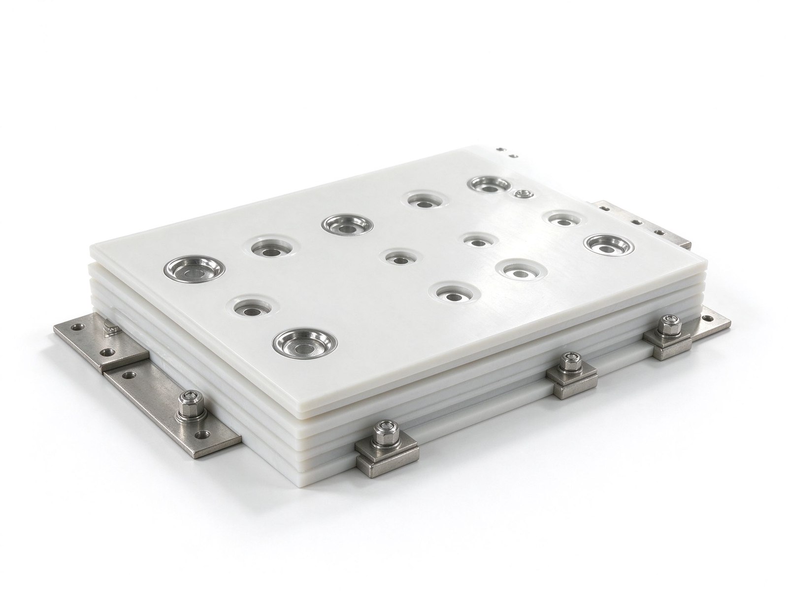
The practical consequence is that AC resistance in a tightly coupled pair can be several times the DC value at switching frequencies, even when the total cross-section is generous. The penalty is usually acceptable at 4-8 kHz IGBT switching, but becomes material at the 20-50 kHz where SiC runs.
In the high-frequency region above a few megahertz, skin and proximity effects exponentially limit the cross-section available to current, and the AC resistance R increases dramatically because resistance is inversely proportional to the effective conducting area (Mitsui et al., IEEE, 2021). The same study showed the practical upside: an optimised laminated busbar geometry reduced surge voltage by 13.2%, damped oscillation by 49.7% and switching loss by 29.7% simultaneously in a 400 V / 30 A buck converter, relative to design objectives.
The message is that AC resistance is designable. Laminate thickness, inter-plane spacing, layer order and terminal placement are all levers, and they are levers a FEM solver can turn before copper is cut.
Multiple thinner laminated bars in parallel - spaced and insulated rather than one thick solid bar - increase the surface-area-to-volume ratio and keep each lamination's thickness closer to the skin depth (WAZIPOINT, July 2026). Each thin layer carries its share of current across its full cross-section instead of wasting its centre, and the layers' surfaces add to the total conducting perimeter.
This is the laminated busbar's decisive advantage at frequency: the stack of thin layers is both a low-inductance structure and a low-AC-resistance structure, because the same geometry that cancels loop inductance also multiplies conducting surface.
For very high current EHV substation applications - GIS and AIS busbars above roughly 3,000-4,000 A - hollow tubular conductors are the classic answer, because the conductor core carries negligible current at power frequency and the tube removes the dead copper (WAZIPOINT, 2026). In power-electronics cabinets, the equivalent move is to keep laminate layers thin and numerous rather than thick and few.
The crossover between solid, tubular and laminated is set by current level, frequency and mechanical duty. The ampacity chart gives the DC basis; this guide adds the frequency correction.
Because high-frequency current concentrates on the surface, surface quality matters disproportionately at joints. Tinned or silver-plated surfaces at connections keep the high-current-density outer skin on a low-resistance finish, and plating thickness uniformity becomes an electrical specification, not a cosmetic one. A 3-10 um tin plating per ASTM B545, written as a local minimum on contact areas, is the practice we apply at SHANYUAN (see our plating and corrosion guide).
Silver plating is the higher-performance choice for high-cycle power contacts; nickel adds corrosion resistance in humid cabinets. The plating decision belongs in the design review, with the skin-depth argument on the table.
One caution on plating at frequency: the finish that wins on DC contact resistance is not automatically the finish that wins on AC. At DC, the plating's job is contact surface; at frequency, the skin effect forces current through the outer finish, and a finish with higher resistivity than the base metal adds loss in the skin layer even when its contact resistance is excellent. The engineering answer is to specify the finish thickness and resistivity alongside the DC contact requirement, and to verify the assembly's AC behaviour in the impedance sweep rather than assuming the DC resistance measurement tells the whole story.
In practice, silver plating on copper is the high-frequency-friendly choice because its resistivity is close to copper's; tin plating, the workhorse for DC bolted joints, is slightly worse at frequency but entirely acceptable when the skin depth at the switching frequency is large relative to the plating thickness - which is true for most industrial switching frequencies and false at tens of MHz. The check is a two-line calculation that belongs in every high-frequency design review.
If you simulate a busbar at frequency, the mesh must resolve the skin depth or the answer is wrong. The rule used by CAE vendors: at least three or more element layers within the skin depth. At 20 kHz, delta = 0.47 mm, so you need element sizes of 0.15 mm or less within 0.47 mm of the conductor surface, while the conductor centre carries almost no current and can use a coarse mesh (NovaSolver, 2026).
This is why frequency-domain AC resistance and inductance results should be taken seriously only from a converged mesh, and why 'quick estimate' tools that ignore proximity systematically understate loss in tightly coupled DC-links. The full simulation workflow, from partial-inductance math to double-pulse validation, is in our FEM impedance simulation guide.
The laminated busbar solves both problems with one geometry. Loop inductance is minimised by making the forward and return planes close and wide; AC resistance is minimised by keeping each layer thin relative to skin depth and multiplying surface. The inter-plane dielectric thickness trades capacitance against inductance: thinner film means lower inductance and higher parasitic capacitance; thicker film the reverse. That trade is a design decision for the switching waveform, not a default.
SHANYUAN's multi-layer laminated busbar family is built for exactly this trade, with layer count from 2 to 6+ and film choice in PET, Nomex or DLF.
One more effect belongs in the layer discussion: the capacitive side. The close spacing that wins on inductance and AC resistance also creates inter-plane capacitance, and that capacitance forms the common-mode path that conducted EMI follows. The design trade is therefore three-way - inductance, AC resistance and capacitance - and the laminate's inter-plane film thickness is the single knob that moves all three. The resonance formed by the laminate's inductance and its capacitance sits somewhere above the switching band for a well-designed part; a resonance inside the band is a design error that the impedance sweep will find and that the converter's EMI filter design should know about.
The EMI argument strengthens the case for getting the geometry right in simulation. The common-mode current driven by the switching dv/dt flows through the laminate's parasitic capacitance into the heatsink and the chassis, and the grounding strategy - where the laminate connects to the chassis, and through what impedance - is part of the busbar design file, not a downstream filter problem. Our low-inductance design guide covers the geometry side; the frequency side is this guide's subject.
The proof of a low-inductance, low-AC-resistance busbar is measured, not simulated. Double-pulse testing on the actual converter quantifies the voltage overshoot and switching energy; impedance analyser sweeps from 1 kHz to tens of MHz capture the resistance rise and the parasitic resonance. The IEEE literature validates analytical partial-inductance methods against 3D FEM and against double-pulse tests on 3.3 kV SiC MOSFET converters (IEEE Xplore, 2026) - the same three-way verification we recommend for traction-grade parts.
Three rules cover most designs. Up to 1 kHz, treat DC resistance as the design basis and focus on thermal sizing. From 1 kHz to the switching frequency, check the ratio of layer thickness to skin depth - keep each layer at or below about 2 x delta. Above the switching frequency, expect AC resistance to dominate and drive the laminate count and spacing rather than the total copper mass. When in doubt, simulate with a converged skin mesh, then measure.
The rules of thumb hold across a wide range of hardware, and one more boundary deserves a line: they apply to the busbar itself, not to the connectors and cables feeding it. A bolted joint to a cable lug brings its own high-frequency behaviour - the lug's geometry, the bolt's material and the plating all sit in the same current path - and the skin-depth logic that governs the bar governs the lug equally. The cleanest designs treat the whole current path, from laminate to terminal to lug, as one frequency-domain object, which is why the impedance sweep is taken across the assembly rather than the bar alone.
The patterns matter most where switching is fastest: SiC traction inverters, solar string inverters and fast chargers. In each, the DC-link commutation loop is a few centimetres, the laminate is two to six layers, and the AC-resistance loss at switching frequency is a line item in the efficiency budget. The same laminated geometry that keeps the loop at tens of nanohenries keeps the AC loss to watts rather than tens of watts. Our inverter DC-link busbar and power-electronics laminated busbar pages describe the build patterns.
Final checklist for a high-frequency busbar: know the switching frequency and its harmonics; compute skin depth and keep layer thickness near or below 2 x delta; run the proximity-effect check on the coupled pair; specify surface finish and plating for the current-carrying skin; mesh the simulation to resolve the skin depth; verify with double-pulse and impedance sweep; and freeze the geometry against the enclosure's thermal budget. Our engineering desk can run this checklist against your profile - send the frequency, current and envelope, and the sizing returns with the quotation.
A real switching waveform is not a single sine at the switching frequency - it is a pulse train whose spectrum carries energy at the switching frequency and its harmonics, plus the di/dt spike energy that extends to the tens of MHz. The busbar sees the sum: the fundamental switching frequency sets the dominant AC-resistance component, but the harmonic content up to the device's rise-time bandwidth adds loss where the skin depth is a fraction of a millimetre.
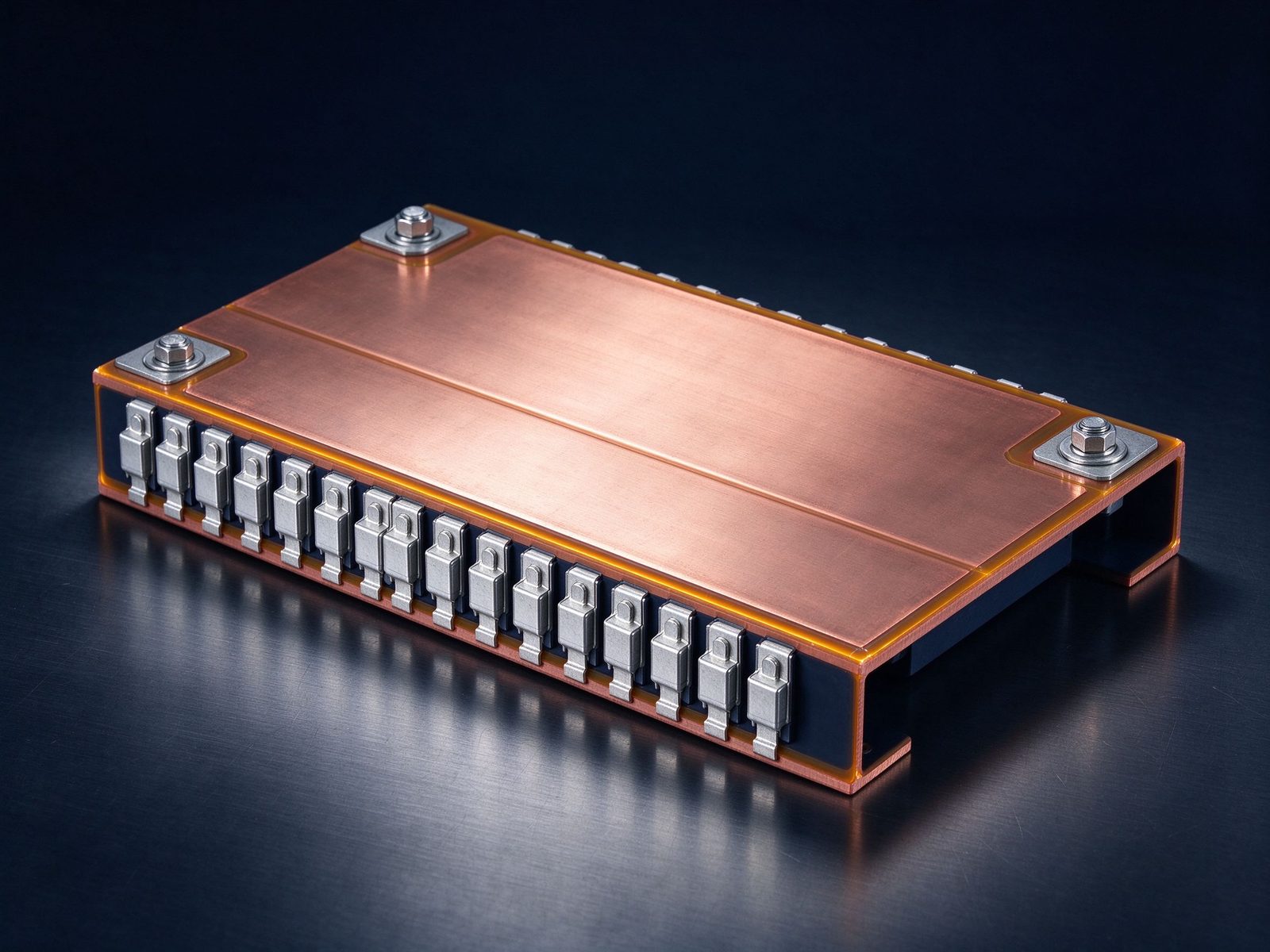
The honest treatment is a spectrum-based loss calculation: take the measured or simulated current waveform, decompose it, and sum the I2R loss per harmonic using the frequency-dependent resistance. For SiC systems this can double the apparent AC loss versus a single-frequency estimate - which is why 'the switching frequency number' is never the whole story.
Not all 'laminated' busbars are equal at frequency. A bonded stack - layers pressed and bonded into one rigid body - behaves electromagnetically as a single structure with the layer pattern fixed; a loosely layered or taped assembly can have different current distribution because layer-to-layer contact varies. The distinction matters in the loss calculation and in repeatability: the bonded stack's AC resistance is a manufactured property, repeatable part to part, while a loose stack's is a field variable.
This is one reason SHANYUAN's stacks are one-pass bonded into a single component: the electrical performance is set in the lamination press, not left to assembly. The manufacturing detail is described in our manufacturing process guide.
The impedance analyser gives the frequency-domain truth of the busbar: inductance and resistance sweeps from 1 kHz to tens of MHz capture the rise in AC resistance, the self-resonance where the laminate's capacitance meets its inductance, and the effect of terminal geometry. The sweep is the bridge between the FEM extraction and the converter's real behaviour - it validates the model at frequencies the double-pulse test only samples indirectly.
The measurement protocol matters: fixture inductance must be subtracted (or the measurement made in a calibrated fixture), the sweep should run on the production part, not a prototype, and the resonance frequency should be compared with the converter's excitation content. A resonance inside the switching band is a design error that no solver would miss but that only measurement confirms has been fixed.
Take a SiC DC-link switching at 50 kHz with a di/dt spike band out to 30 MHz. Skin depth in copper is 0.30 mm at 50 kHz and 0.12 mm at 300 kHz - the fifth harmonic. A 3 mm solid bar at 300 kHz has an effective conducting layer about 0.1 mm thick per face: the AC resistance is roughly three to five times DC. The same current on a three-layer stack of 1 mm layers, each close to the skin depth at 50 kHz, stays within about 1.5 times DC.
That ratio is the entire argument for thin, parallel layers in high-frequency service: the loss difference between the solid bar and the stack is a line item in the converter's efficiency budget, and at 100 kW it is watts that become heat. The geometry rule - layer thickness near or below two skin depths at the switching frequency - is the one number to take away, and it applies just as much to the kiloamp DC buses of electrolyzer plants as to inverter cabinets.
Conductor material choice interacts with frequency more than with DC. Copper's resistivity is about 1.7e-8 ohm-m at 20 °C and rises with temperature; aluminium is about 1.6x higher, which both shortens the skin depth at a given frequency and raises the AC resistance at the same geometry. Plating has a double role: it carries the current at the surface where the skin lives, and its resistivity relative to the base metal sets how much of the AC current actually flows in the finish. Silver plating, with resistivity close to copper's, is nearly transparent at frequency; a poorly applied thick plating with high contact resistance is the opposite.
The design rule: specify the finish for the frequency, not just for corrosion. The plating and corrosion guide gives the finish selection logic, with the skin-depth argument added on top at high frequency.
The design review for a high-frequency busbar should read like a checklist, not a conversation. Is the switching frequency and its harmonic band defined? Is each layer thickness at or below about two skin depths at the switching frequency? Has the proximity effect been checked on the coupled pair - including the neutral plane in multi-level topologies? Is the plating specified for the current-carrying surface with a documented minimum? Has the simulation mesh resolved the skin depth, and does the convergence study hold? Has the resonance frequency been compared with the switching band? And does the double-pulse or impedance-sweep evidence match the model?
Each item has a number attached, and each number is either in the file or not. That binary check is what separates a busbar design from a busbar drawing.
Send the current profile, voltage class and terminal types — our engineers reply within one business day.