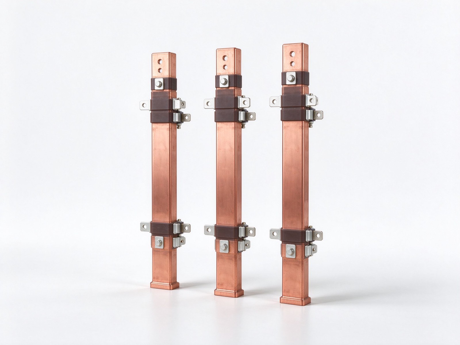
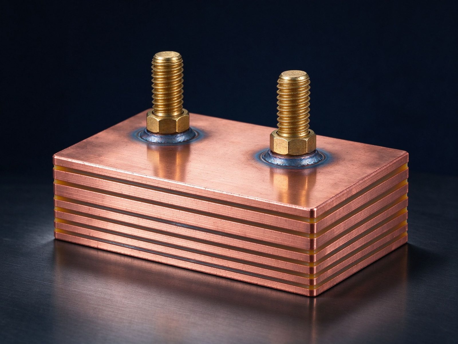
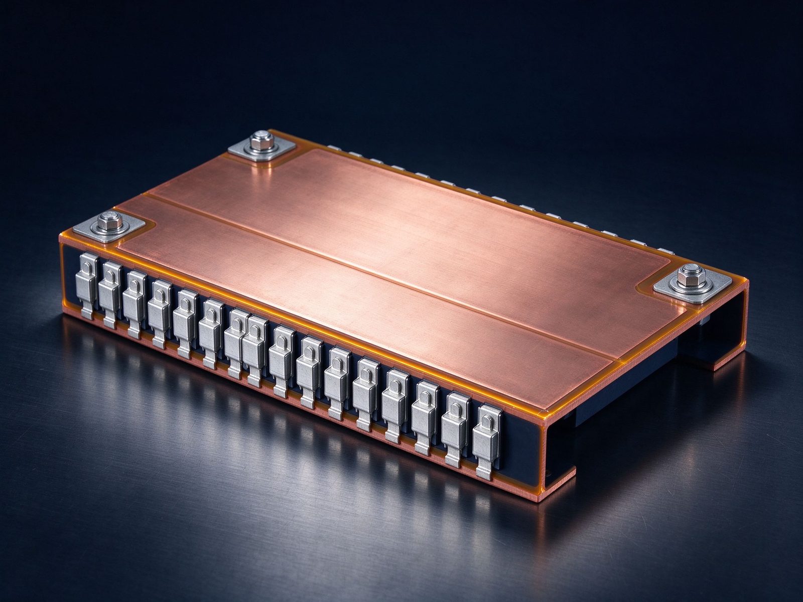
Hot-pressed multi-layer copper sandwich that cancels stray inductance for IGBT and SiC power stages - send a drawing for a quote.
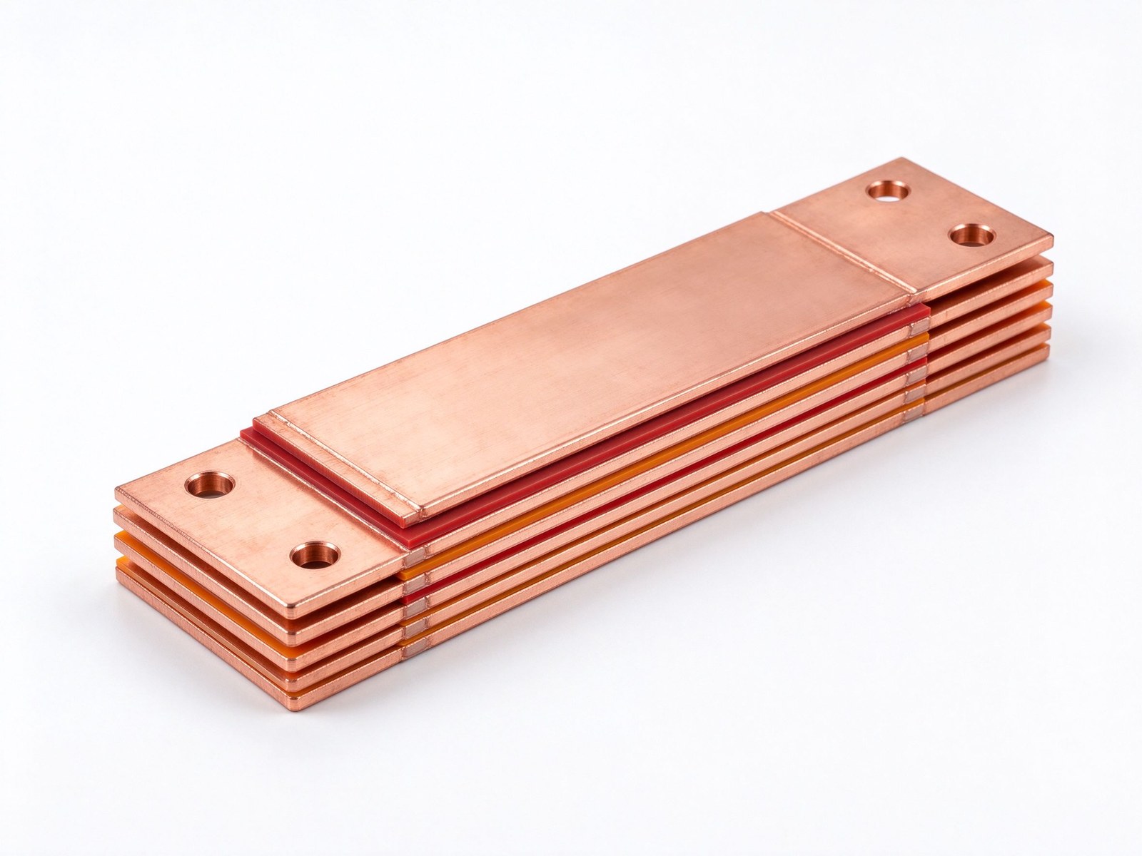
Product imagery: factory photo plus studio renders. The exact geometry, layers and terminals of your part follow your drawing.
Final values follow your drawing — this is the standard configuration of the family.
| Parameter | Value |
|---|---|
| Conductor | C11000 copper, aluminium optional |
| Layer count | 2 to 6+ copper layers |
| Dielectric gap | 5-10 mil films between conductors |
| Dielectric options | FR-4, Mylar (PET), Teonex (PEN), Nomex, Kapton, epoxy powder |
| Current rating | Up to ~1,000 A per assembly |
| Edge treatment | Open, pinched or epoxy-filled |
| Factory test | 100% hi-pot withstand + partial discharge |
| SKU | SY-PE-215 |
Key characteristics of this product family.
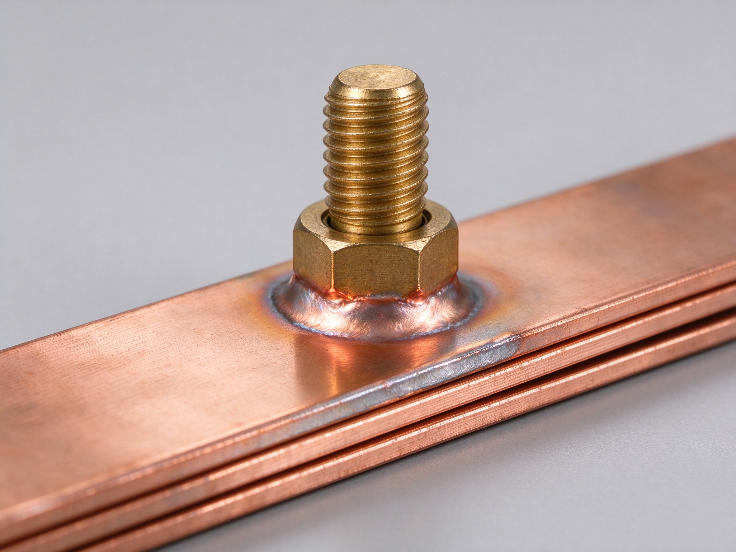
A laminated copper busbar stacks two or more copper conductor layers across very thin dielectric films, then hot-presses the whole sandwich under heat and pressure into one rigid, integrated part. There are no hand-wrapped tapes and no loose cable harness inside - the assembly arrives pre-built, drilled and ready to bolt into the cabinet.
The performance advantage lives in the 5-10 mil dielectric gap. With DC+ and DC- conductors running face to face across that gap, their magnetic fields overlap and cancel - mutual inductance cancellation - and the stray loop inductance collapses to single-digit nanohenries. That is exactly what fast-switching IGBT and SiC stages need: lower switching overshoot across the semiconductors, reduced diode-recovery stress, a stiffer DC-link voltage and fewer snubber components. It is why this construction is the standard feed for traction inverters, solar and wind converters and UPS power stages, where the goal is clean, switch-friendly power.
Reliability improves the moment the layers fuse during lamination. The stack behaves as one piece under vibration, with none of the relative movement that fatigues taped cable bundles. Every laminate leaves production after a 100% hi-pot dielectric withstand test and a partial-discharge check, so leakage performance is verified on each part rather than assumed from the batch.
Thermally, tight stacking frees cabinet airflow and lets conductor sections be sized precisely instead of over-built; where natural convection is not enough, an aluminium layer with machined channels can be laminated straight in as an integrated cold plate. The cut edges are treated three ways: open edge for dry controlled cabinets, pinched edge for dust and light moisture, or epoxy-filled edge for humid, contaminated and wash-down environments.
Every switch transition in a power loop dissipates energy stored in stray inductance as voltage overshoot: V = L x di/dt. A laminated busbar collapses L by running the DC+ and DC- planes face to face across a 5-10 mil dielectric film, so the loop area shrinks and the overlapping magnetic fields cancel each other. The result is single-digit-nanohenry loop inductance without extra snubber capacitors. Our low-inductance design guide shows the loop-area math; for the capacitor side of the same loop see the capacitor bank busbar and inverter DC-link busbar pages.
Pick the inter-layer film by continuous temperature, dielectric constant (ASTM D150), dielectric strength (ASTM D149) and UL 94 flammability:
| Dielectric | Max cont. temp | Diel. const. D150 | Diel. strength D149 | Flammability |
|---|---|---|---|---|
| FR-4 / glass-epoxy | 140 C | 4.3 | 1,250 V/mil | UL 94 V-0 |
| Mylar (PET) | 105 C | 3.3 | 7,500 V/mil | UL 94 VTM-0 |
| Tedlar (PVF) | 105 C | 11.0 | 3,500 V/mil | UL 94 HB |
| Teonex (PEN) | 140 C | 3.4 | 5,000 V/mil | UL 94 VTM-0 |
| Nomex | 220 C | 1.6 | 430-845 V/mil | UL 94 V-0 |
| Kapton (polyimide) | 400 C | 3.7 | 5,000 V/mil | UL 94 VTM-0 |
| Epoxy powder coat | 130 C | 4.0 | 800 V/mil | UL 94 V-0 |
Nomex and Kapton serve high-temperature drives; PET is the cost-controlled choice for room-temperature inverters; FR-4 and epoxy powder add rigidity and a V-0 rating. See busbar insulating films.
The cut edge decides long-term life in your environment:
For heat beyond natural convection, we laminate an aluminium cold plate with machined coolant channels straight into the stack - see thermal management. Hi-pot and leakage checks are explained at partial discharge testing. Send a drawing through the custom busbar design service.
A laminated copper busbar cancels inductance by running conductors face to face across a thin dielectric; the number of layers and the dielectric gap set how far that cancellation goes. Values below are planning estimates for a hot-pressed C11000 stack quoted across industrial, inverter and traction use, assuming a 300 mm run unless noted.
| Stack Configuration | Dielectric Gap | Stack Length (typ.) | Loop nH | 800 V Rail Spike (est.) |
|---|---|---|---|---|
| Single layer, no lamination | Air gap above 20 mm | 300 mm | 80–120 nH | ≈ 220–340 V |
| Two-layer face-to-face laminate | 0.18 mm PET | 300 mm | 18–28 nH | ≈ 50–80 V |
| Three-layer laminate, common return | 0.20 mm Nomex | 240 mm | 10–16 nH | ≈ 25–42 V |
| Low inductance laminated busbar, four-layer | 0.15 mm epoxy film | 200 mm | 6–10 nH | ≈ 16–30 V |
| Capacitor-sandwich four-layer stack | 0.15 mm film | 150 mm | 4–8 nH | ≈ 12–24 V at fast edge |
These numbers are planning estimates for a tin-plated C11000 stack; the spike column follows ΔV = L × di/dt with the edge rate planned between 1.5 and 3 A/ns depending on device family. Laminated busbar dielectric materials are chosen for the voltage class and operating temperature — PET up to around 130 °C continuous, Nomex for higher temperature, epoxy film for the tightest gap. Laminated busbar edge sealing is what keeps the dielectric out of moisture and contamination, and a well-sealed stack typically meets the humidity class the enclosure calls for. The low-inductance busbar design notes explain the gap-versus-nH relationship, and the dielectric selection guide compares the film options.
Because a laminated copper busbar is a generic build rather than a dedicated DC link, the terminal geometry can be cut to a wide range of module and device packages. The list below is the broader package families we routinely tool laminated tabs for, with the terminal patterns most often specified across industrial, renewable and traction builds; tab current density is planned near 1.0 A/mm² continuous.
| Module Package Family | Terminal Pattern | Tab / Blade Spec We Tool | Typical Use |
|---|---|---|---|
| EconoPACK 4 | AC and DC screw lugs | M5–M6 tab, 15–25 mm pitch | Industrial drives |
| SEMiX 5 | Spring terminals | Low-profile blade, 10–18 mm | Renewable converters |
| HP1 | Press-fit pins | Pin-grid blade termination | Traction laminates |
| SKiiP 4 | Integrated busbar studs | Custom blade to stud drawing | High-duty drives |
| PrimePACK 1 | Screw terminals | M6 blade set, 30–50 mm pitch | Wind and traction converters |
| flow 1 | Screw or pin terminals | M4 blade on 10–18 mm pitch | Compact onboard inverters |
Quote us the module datasheet; the DFM step locks tab width, pitch and stand-off height against that drawing. Where the terminal lands on a non-module device — a capacitor, a fuse or a terminal block — we tool the tab to that device drawing instead. Plating on the tab face is tin as standard, with silver on request for higher-pressure joints. The custom design process page describes the review cycle, and the laminated busbar design guide lists the stack and gap options available at tooling. Conductor thickness is typically 0.5 to 2 mm per layer, and a two-layer stack is the default when the current rating stays below about 400 A per phase. A three-layer stack is quoted when the rating climbs toward 800 A, and a four-layer sandwich is the typical choice above 1000 A per phase or for fast-edge duty.
Where this busbar configuration earns its place.
Where this busbar configuration earns its place.
Where this busbar configuration earns its place.
Where this busbar configuration earns its place.
Where this busbar configuration earns its place.
Where this busbar configuration earns its place.
Your drawings reach the engineers who build the part.
Design risks flagged when changes are cheap.
Test records per lot, CoC and PPAP on request.
Drawing to delivered production parts, one supplier.
From spec review to shipped, tested parts — one accountable supplier.
Straight answers from the engineering team.
Every SHANYUAN busbar is custom, but the power circuits they connect recur across markets. Three typical ones — send us yours and we will point to the right stack-up.
Tight, low-inductance links between the battery source and traction inverters, fully edge-sealed for 400–800 V platforms.
Commutation-loop connections from DC-link capacitors to IGBT bridges, designed against switching overshoot V = L × di/dt.
Converter DC links built for rising bus voltages toward 1500 VDC, with creepage and partial-discharge margins included.
Construction, dielectric selection and current capacity basics.
Read the busbar design guideLayers, terminals, dielectrics and mounting are all configurable. Send us your spec for DFM review and a quotation within one business day.