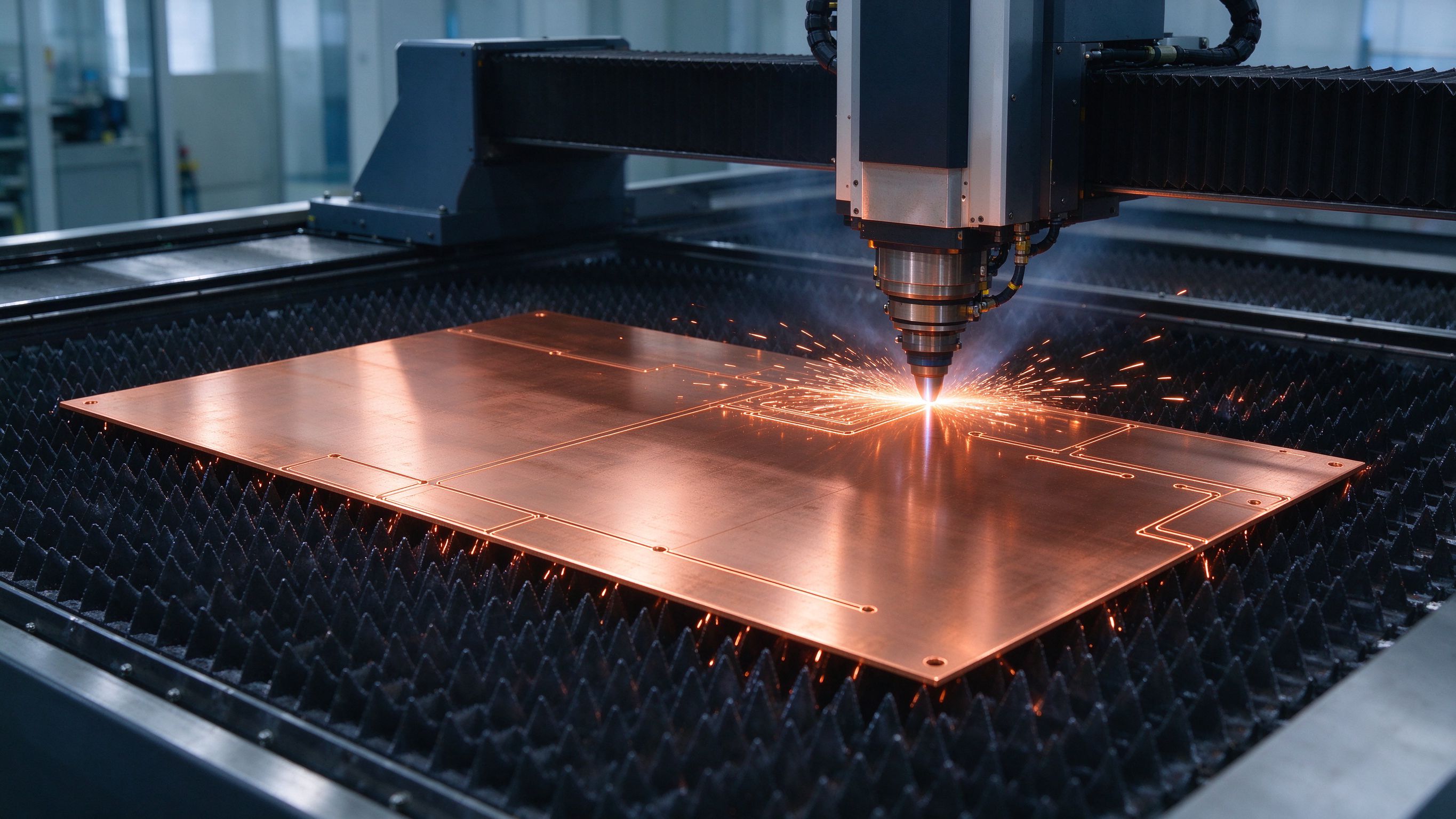
In the commutation loop of an inverter, every nanohenry counts. Laminated busbars cut loop inductance to keep switching devices inside their safe operating area.
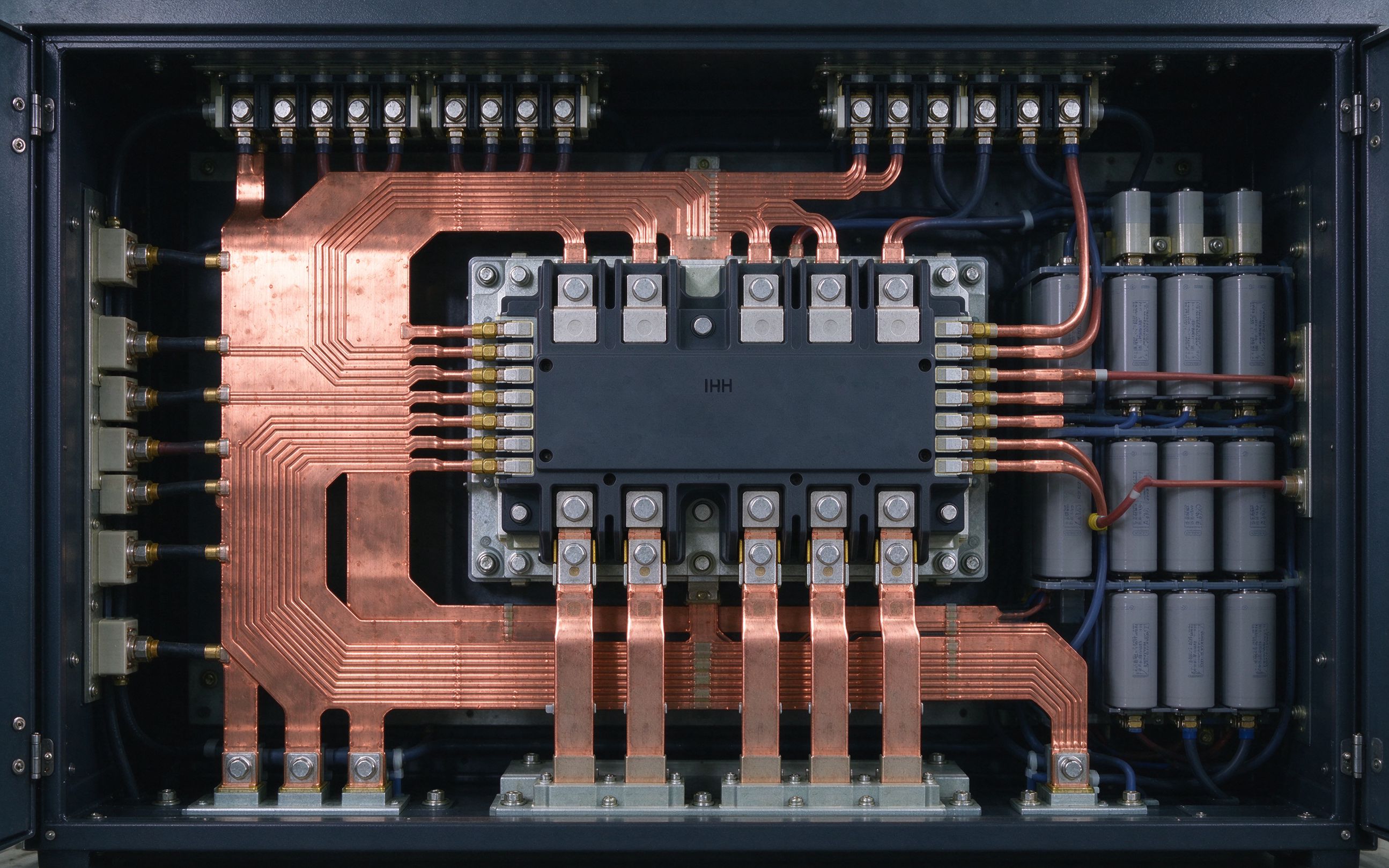
The four places busbars carry current in this application.
The laminated connection between the capacitor bank and the inverter bridge.
Matched busbar sets with blade terminals at module pin pitch.
Multi-tab laminates sharing current evenly across parallel capacitors.
Compact, fully insulated assemblies for high-voltage platforms.
Low-inductance DC links for double-conversion UPS protecting critical loads.
Form-fitting output bars routing the bridge outputs to the filter stage and terminal block.
Layer count and conductor width tuned with your DC link capacitor placement.
Standoff and creepage reviewed for your voltage class.
Terminal pitch matched to module datasheets to avoid adaptation hardware.
SiC and GaN switching benefit most from low-inductance DC links.
IGBT, SiC or GaN and the switching frequency define how aggressive the inductance budget must be.
New power architectures — EVs, consumer electronics, renewables — keep expanding the use of AC-DC and DC-DC converters and DC-AC inverters. Designs push switching frequencies higher to shrink size and save board space, which makes thermal management an increasing challenge, while the converter location is often extremely space-limited. In the commutation loop of any inverter, every nanohenry of stray inductance shows up at switch-off as voltage overshoot: V = L × di/dt. That overshoot drives power component ratings, switching frequency and losses, which is why the DC link is designed around the busbar.
A laminated busbar is built for exactly this. Inductance of a conductor depends on its shape and the proximity of opposite current paths; the lowest-inductance geometry is given by parallel planes — the structure of a laminated busbar. To minimize inductance, opposing conductors are brought extremely close, with reference designs holding dielectric spacing under 100 µm between opposing layers. The busbar distributes current from the DC-link buffer capacitors to the IGBT/MOSFET modules through defined, low-inductance paths, and soldering or bolting capacitors as close as possible to the device terminals eliminates the long individual leads that would otherwise extend the commutation loop.
Partial discharge is the second control axis, especially as bus voltages climb. Trapped air bubbles at insulation-to-conductor and insulation-to-insulation interfaces initiate PD; production verification keeps it below the industry reference level of 10 pC, even at test voltages above the operating voltage. We walk through both control axes in our engineering notes on low-inductance busbar design and on partial discharge in busbars.
Where the current sits between a PCB and a full laminated bar — roughly 100–500 A — reference designs use thick-copper hybrid construction (400–800 µm copper), wave-solderable like a PCB while carrying busbar-level current. We build these DC links as 1–6+ layer C11000 copper assemblies, tin-plated and edge-sealed, part of our power electronics busbars family; the same low-inductance, PD-controlled geometry carries over to aerospace converter DC links when platforms move into airborne or defense environments. Every DC link ships with lot-by-lot hipot, PD and dimensional test records. Send us the module datasheet and capacitor layout — DFM review within one business day.
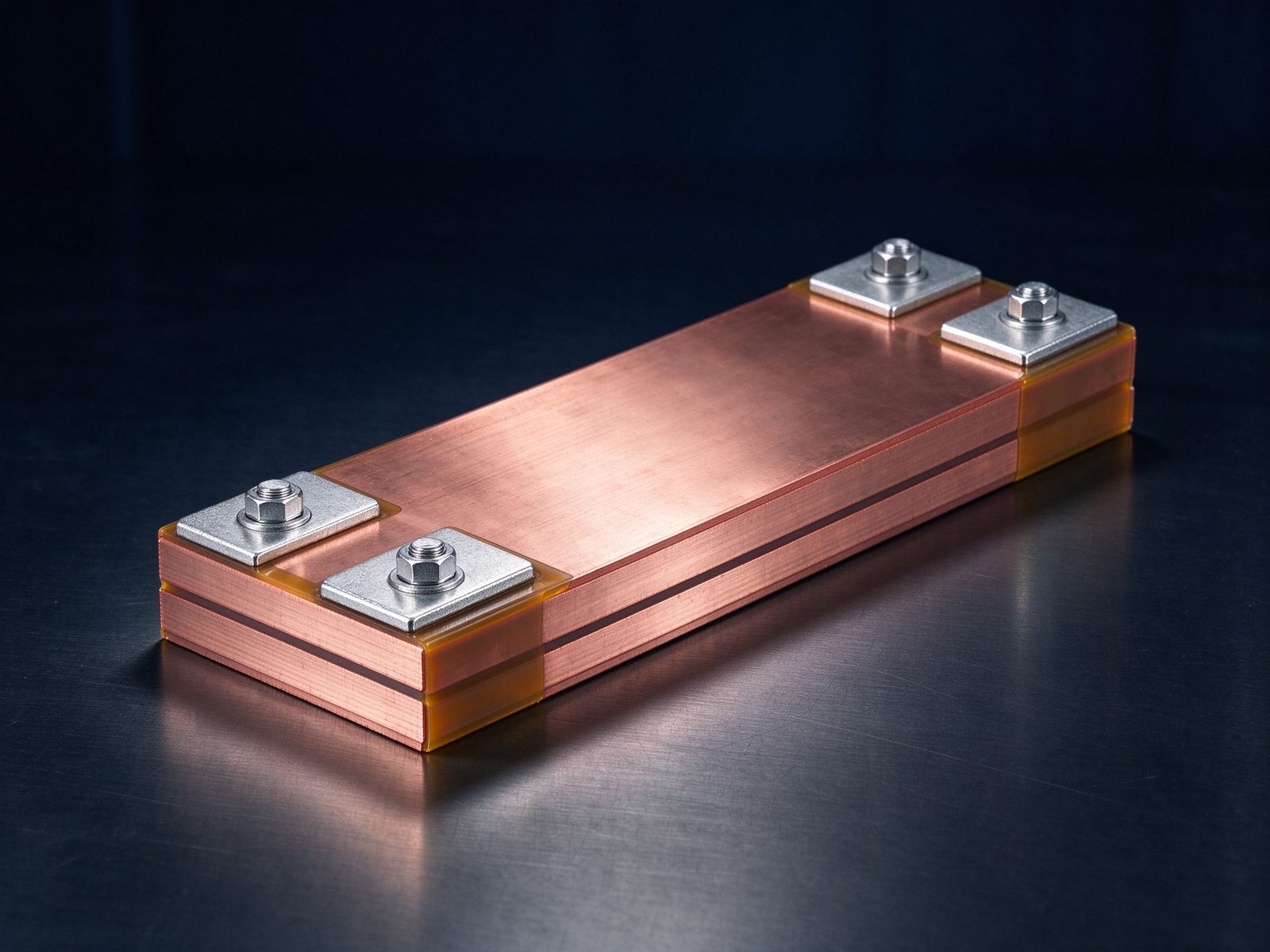
The part this application is built around — a SHANYUAN laminated busbar, factory direct.
Ảnh tham chiếu từ sản xuất SHANYUAN và các cụm lắp ráp đã xuất.
Các ghi chú và trang sản phẩm chọn lọc hỗ trợ các quyết định thiết kế trên trang này.
Các dòng thanh cái phù hợp đáp ứng biên độ dòng của ứng dụng này.
Thanh cái DC link ép lớp dài với đầu nối chân phẳng cho thiết kế biến tần độ tự cảm thấp.
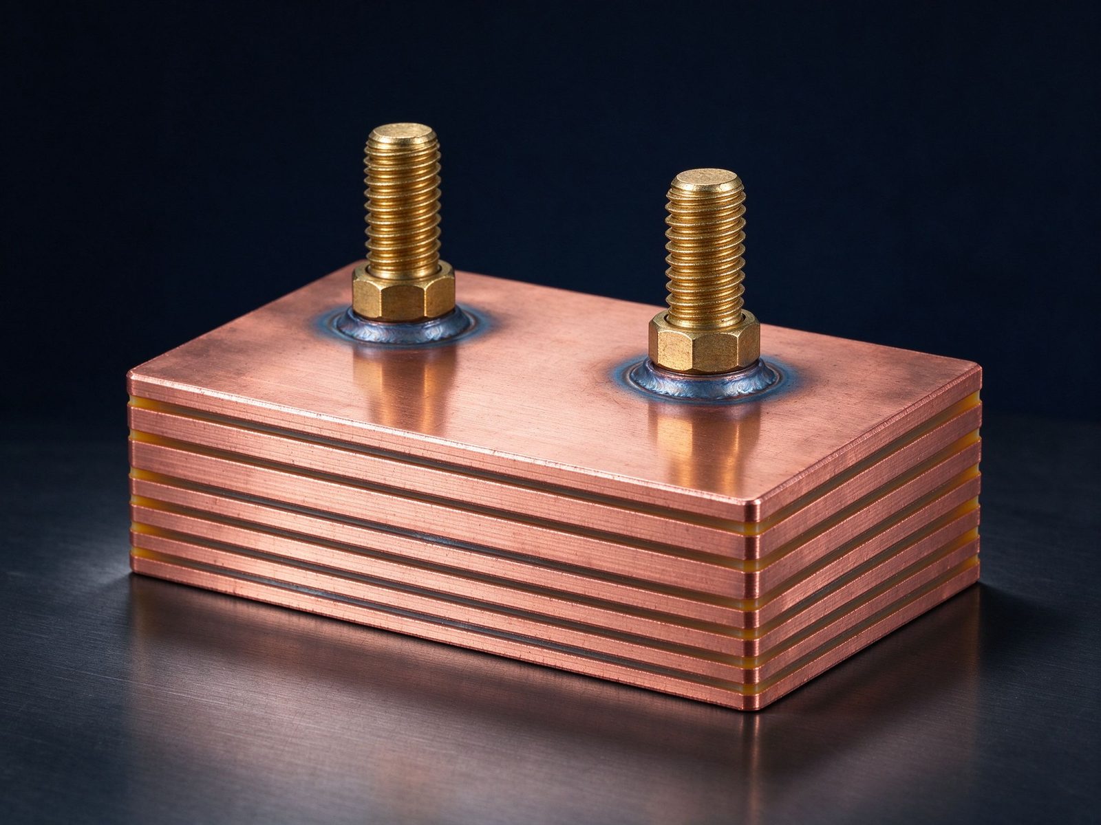
Cụm thanh cái ép lớp hàn để phân phối điện dòng cao với các chân đã hàn sẵn.
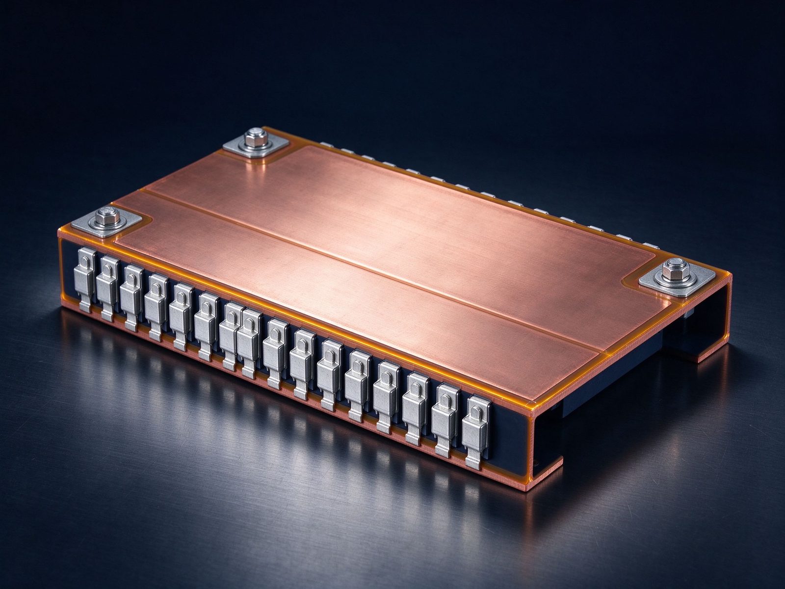
Thanh cái ép lớp cho biến tần truyền lực EV với đầu nối chân phẳng cho kiến trúc cao áp.
Từ rà soát thông số đến linh kiện giao hàng và kiểm thử – một nhà cung cấp chịu trách nhiệm.
| Material | Standard options |
|---|---|
| Conductors | C11000 copper as standard; aluminum available on request |
| Dielectrics | PET, Nomex and epoxy (DLF) films, selected by voltage class and operating temperature |
| Plating | Tin finish for corrosion protection and joint solderability |
Cấu trúc, chọn điện môi và cơ bản về khả năng dòng.
Đọc hướng dẫn thiết kếVoltage class, current profile and terminal types — we will share reference configurations and DFM guidance.
Câu trả lời thẳng thắn từ đội kỹ thuật.
Send the application, voltage class and current profile — we will share reference configurations and DFM guidance.